Introduction
Rework in PCB production often stems from defects that escape initial inspections, leading to substantial financial losses and extended timelines for electric engineers managing high-stakes projects. Design for Testing (DFT) emerges as a critical methodology to preempt these issues by embedding testability into the PCB layout from the outset. This ensures compatibility with essential PCB testing methods like flying probe testing, in-circuit testing (ICT), and automated optical inspection (AOI), all while maintaining IPC compliance. Engineers benefit from reduced scrap rates and faster time-to-market when DFT principles guide the design process. Ultimately, these strategies align production with quality benchmarks, safeguarding reliability in demanding applications.
What Is Design for Testing (DFT) and Why It Matters
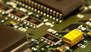
Design for Testing (DFT) refers to a set of intentional design choices that enhance the ability to verify PCB integrity through automated and manual tests. It focuses on improving accessibility for probes, cameras, and fixtures, targeting common failure modes such as opens, shorts, wrong component values, and polarity errors. In the context of IPC compliant PCBs, DFT bridges design and manufacturing, ensuring boards meet performance specifications without excessive post-production fixes. Without DFT, testing becomes inefficient, probing times skyrocket, and yield drops, amplifying costs exponentially in high-volume runs.
The relevance of DFT intensifies for electric engineers handling complex multilayer boards where hidden defects lurk beneath components or dense routing. Industry data underscores that early DFT integration can cut testing expenses by optimizing fixture development and probe paths. IPC compliance standards further elevates DFT's value, as it standardizes test point placement and net accessibility. Factory insights reveal that DFT-compliant designs facilitate seamless transitions between prototyping and mass production, minimizing variability across batches.
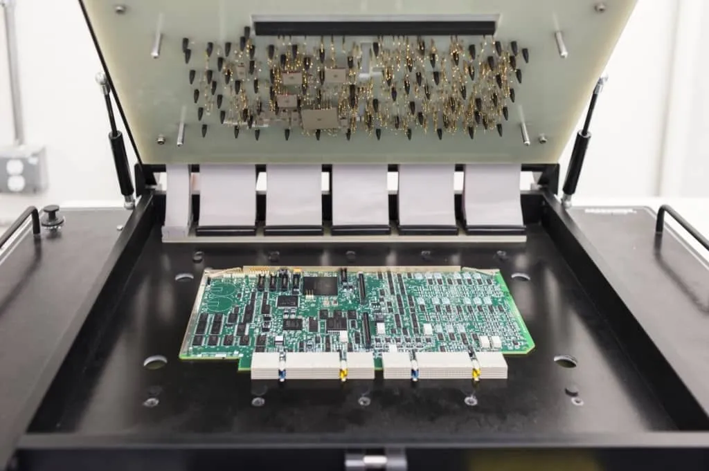
Key PCB Testing Methods and Their DFT Requirements
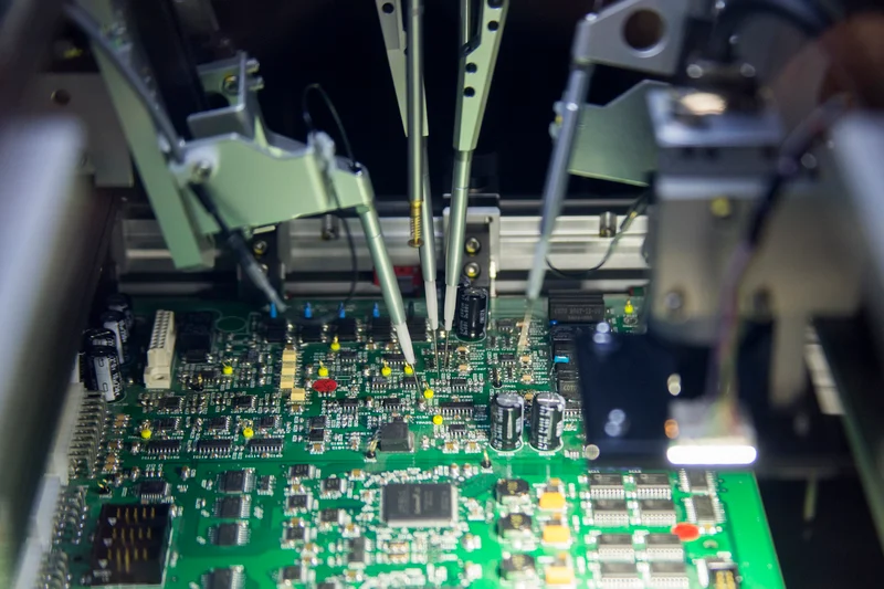
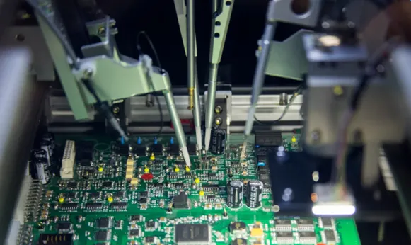
PCB testing methods form the backbone of quality control, each demanding specific DFT features to operate effectively. Flying probe testing uses movable probes to contact test points, making it ideal for low-volume or prototype boards due to its fixtureless setup. This method excels at detecting electrical continuity and isolation but requires unobstructed access to at least 90% of nets for optimal coverage. DFT strategies must prioritize probe-friendly pads, avoiding clustering or placement under tall components that could hinder movement.
In-circuit testing (ICT), conversely, employs a bed-of-nails fixture pressing against fixed test points for high-speed parallel measurements. It provides comprehensive functional checks on populated boards, including component values and solder joints, but demands precise fixture design tied to DFT layouts. Electric engineers favor ICT for medium-to-high volumes where speed trumps setup flexibility, yet poor DFT can lead to fixture redesigns costing thousands. Ensuring 100% net access and standardized spacing prevents such pitfalls.
Automated optical inspection (AOI) complements electrical tests by visually scanning for assembly defects like missing parts or bridges using high-resolution cameras. While non-contact, AOI relies on DFT elements such as fiducials for alignment and clear zones around components for accurate imaging. Integrating these methods through DFT creates a layered verification approach, catching issues at bare board, assembly, and functional stages.
Technical Principles of Effective DFT Implementation
At its core, DFT hinges on principles of observability and controllability, ensuring every net can be stimulated and measured without interference. Test points, typically 0.8mm to 1.0mm diameter pads, must be routed to every node, preferably on the board's bottom side to avoid component shadows. Spacing between adjacent points should exceed probe tip separation, often around 2.54mm, to accommodate standard fixtures in flying probe or ICT setups. Guard traces or rings around high-voltage nets prevent arcing during tests, a factory-driven insight for maintaining IPC electrical test integrity.
Component orientation plays a pivotal role, with polarized parts aligned consistently to simplify ICT programming and reduce fixture complexity. Vias serving dual purposes as test points enhance density without extra real estate, provided they meet via reliability specs. For multilayer boards, blind or buried vias demand careful netlist verification, as inaccessible inner layers complicate flying probe paths. These mechanisms collectively boost test coverage to near 100%, aligning with quality control imperatives.
Boundary-scan techniques, via standards like JTAG, offer an advanced DFT layer for digital ICs, allowing internal chain testing without physical probes. While not universal, integrating scan chains during schematic capture future-proofs designs for evolving test needs. Electric engineers appreciate how these principles scale from simple to high-density interconnects, preserving signal integrity throughout.
Practical DFT Best Practices for IPC Compliant PCBs
Adopting factory-proven DFT best practices starts with netlist-driven placement, generating test points automatically during layout to guarantee coverage. Position probes for power and ground planes at multiple locations, spaced evenly to handle current loads without hotspots. Avoid routing traces under test pads, as this risks probe-induced damage, and incorporate fiducial marks at board corners for AOI and fixture alignment. These steps ensure IPC-9252 compliance for electrical testing of unpopulated boards, streamlining bare board verification.
For populated boards, designate keeper pins or extended leads on critical components to facilitate ICT without desoldering. Maintain clearance zones of at least 2.5mm around test points, free from silk screen or solder mask overhangs that could foul probes. In high-density designs, prioritize bottom-side access and use teardrop pads to enhance mechanical strength under probe pressure. Referencing IPC-A-600 criteria for acceptability guides visual DFT elements, ensuring defects remain detectable.
Multiboard panels amplify DFT efficiency by sharing fixtures across arrays, but require consistent edge routing and test point mirroring. Simulate probe paths early using design software to identify collisions, a proactive measure cutting rework by validating accessibility upfront. These practices, rooted in manufacturing realities, yield robust IPC compliant PCBs ready for diverse testing regimes.
Common DFT Pitfalls and Troubleshooting Insights
Even seasoned electric engineers encounter DFT oversights, such as insufficient net access in BGA areas where vias cluster densely. Troubleshooting reveals that fanning out balls to edge-accessible points resolves this, though it demands iterative routing reviews. Another frequent issue arises from mismatched component heights blocking probes; elevating test pads via standoffs or relocating them mitigates this effectively. Factory feedback highlights how ignoring Kelvin connections for low-resistance measurements inflates ICT false positives.
Overcrowded edges complicate flying probe entry, so reserving a 5mm border proves invaluable for swivel maneuvers. For AOI failures, obscured fiducials from panelization errors underscore the need for redundant marks. Addressing these through post-layout audits, aligned with IPC-6012 qualification guidelines, prevents escalation to full rework cycles. Proactive DFT validation checklists, covering coverage metrics and spacing rules, empower teams to preempt issues systematically.
Conclusion
Design for Testing (DFT) stands as an indispensable shield against costly rework, empowering electric engineers to deliver IPC compliant PCBs with unwavering reliability. By mastering PCB testing methods like flying probe testing, in-circuit testing (ICT), and automated optical inspection (AOI), and embedding targeted strategies, designs achieve superior testability and yield. Factory-aligned best practices, from test point optimization to clearance planning, ensure seamless manufacturing flow. Prioritizing DFT not only curbs expenses but elevates overall quality, positioning projects for long-term success in competitive landscapes.
FAQs
Q1: What is Design for Testing (DFT) in PCB design?
A1: Design for Testing (DFT) involves engineering PCBs with features like dedicated test points and accessible nets to support efficient verification. It targets electrical and visual PCB testing methods, reducing defects during manufacturing. For IPC compliant boards, DFT ensures high coverage for flying probe testing and ICT, minimizing rework while upholding standards like IPC-9252.
Q2: How does flying probe testing differ from in-circuit testing (ICT) in DFT contexts?
A2: Flying probe testing uses movable probes without fixtures, suiting prototypes and low volumes with flexible DFT layouts. In-circuit testing (ICT) requires bed-of-nails fixtures for rapid, parallel checks on high-volume runs, demanding precise test point grids. Both rely on DFT for net access, but ICT excels in speed while flying probe offers setup ease.
Q3: Why integrate automated optical inspection (AOI) with DFT strategies?
A3: Automated optical inspection (AOI) detects assembly defects visually, complementing electrical tests in DFT frameworks. It requires clear fiducials and component zones per IPC guidelines for alignment accuracy. DFT enhances AOI by avoiding obstructions, ensuring early catch of issues like bridges or misplacements before functional testing.
Q4: What are essential DFT best practices for IPC compliant PCBs?
A4: Key practices include 100% net accessibility via bottom-side pads spaced at 2.54mm minimum, clearance zones around probes, and fiducials for alignment. Align with IPC-9252 for electrical tests and avoid tall components near points. These steps optimize flying probe testing, ICT, and AOI, boosting yield in production.
References
IPC-9252 — Requirements for Electrical Testing of Unpopulated Printed Boards. IPC.
IPC-2221 — Generic Standard on Printed Board Design. IPC.
IPC-A-600 — Acceptability of Printed Boards. IPC.
IPC-6012 — Qualification and Performance Specification for Rigid Printed Boards. IPC.