Introduction
In PCB design for testability, engineers prioritize features that enable reliable verification of board functionality and quality. Compliance with IPC-TM-650 ensures that printed circuit boards undergo standardized testing to detect defects early in the production cycle. Designing testable PCBs reduces manufacturing risks and supports efficient in-circuit testing, flying probe tests, and boundary scan applications. This approach aligns with design for testability (DFT) guidelines, making it easier to achieve high yields and reliability. Electric engineers benefit from structured DFT practices that integrate seamlessly into the layout process. Ultimately, these strategies bridge design intent with verifiable performance under industry-accepted procedures.
What Is IPC-TM-650 and Why Does Testability Matter?
IPC-TM-650 serves as the comprehensive test methods manual for evaluating printed circuit boards across mechanical, electrical, and environmental attributes. It outlines procedures for assessing continuity, insulation resistance, thermal stress, and more, providing a benchmark for qualification and process control. Without proper PCB design for testability, boards may fail these tests due to inaccessible nets or probe interference, leading to costly rework. Test point placement becomes critical to facilitate direct access during electrical verification, ensuring compliance without design compromises. In high-volume production, DFT guidelines prevent test coverage gaps that could mask assembly defects. By embedding testability early, designers uphold IPC-TM-650 standards while optimizing throughput and fault isolation. For a deeper dive into practical implementation, see our guide on Design for Testing (DFT) Strategies for IPC Compliant PCBs.

Key Technical Principles of Testability in PCB Design
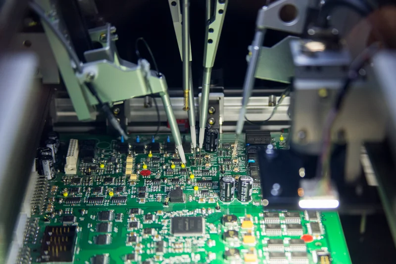
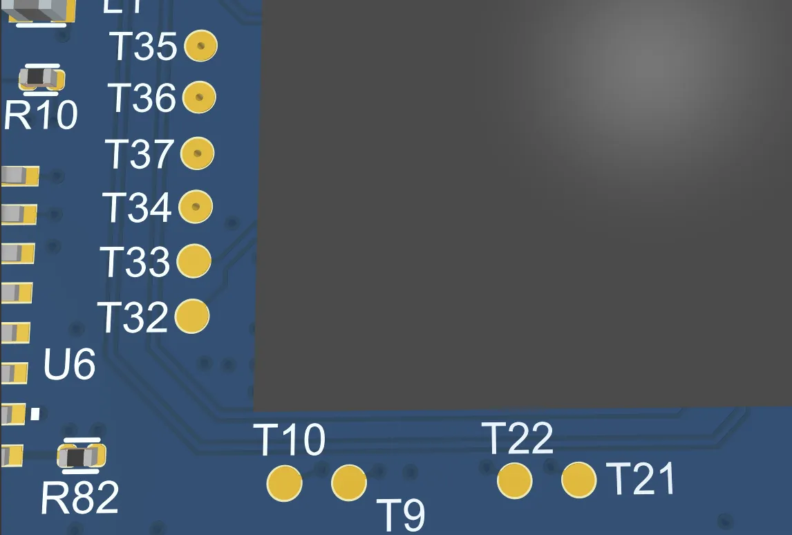
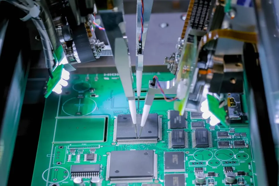
Testability in PCB design revolves around accessibility, probe compatibility, and minimal interference from components or traces. Core principles include dedicating pads or vias as test points on every net, particularly power, ground, and critical signals, to support opens, shorts, and parametric measurements. Spacing between test points must accommodate standard probe sizes, avoiding clustering that could cause crosstalk or physical collisions during automated testing. Component orientation plays a role, with taller parts positioned away from test areas to prevent shadowing in bed-of-nails fixtures. High-density designs require balancing DFT with signal integrity, often using dedicated test layers or edge connectors. These principles ensure that boards meet electrical test requirements without excessive custom fixturing.
Environmental factors influence test point durability, as exposure to thermal cycling or vibration can degrade pad adhesion over time. Engineers must consider solder mask openings around test points to protect against oxidation while allowing reliable contact. For multilayer boards, via-in-pad test points demand precise drilling and plating to maintain continuity under IPC-TM-650 stress conditions. Signal nets at high frequencies benefit from controlled impedance test points to validate performance metrics accurately. Overall, these mechanisms form the foundation for robust DFT implementation.
Best Practices for IPC-TM-650 Design Rules and Test Point Placement
Start DFT during schematic capture by identifying nets requiring test coverage, such as those prone to opens from poor soldering or shorts from bridging. Allocate test points proportionally: one per 50-100 nets for basic continuity, more for complex analog circuits. Place test points on the board edge or component-free zones, maintaining uniform grid patterns for bed-of-nails compatibility. Edge clearance from the board outline should exceed probe radius to avoid delamination risks during fixturing. For flying probe systems, orient points parallel to probe movement paths to minimize travel time.
Incorporate IPC-TM-650 design rules by ensuring test points support dielectric withstand voltage and insulation resistance measurements without disassembly. Use non-plated pads where possible to reduce capacitance effects in high-speed tests, but plated vias for high-current nets. Avoid placing test points under BGA or QFN components, as shadow effects hinder access. Silkscreen labels adjacent to points aid manual probing and documentation. Validate placement through design rule checks that flag violations like insufficient spacing or overlap with keep-out zones. Learn how to optimize fixture design in our ICT Fixture Design Guide: Optimizing PCB Test Coverage.
Layer stackup influences testability, with dedicated inner layers for ground planes improving noise immunity during measurements. For double-sided boards, mirror test points on both sides for comprehensive coverage. High-reliability designs incorporate redundant points for critical functions, ensuring testability post-assembly. Simulate probe contact forces in layout tools to predict pad stress. These practices streamline compliance verification.
Advanced DFT Guidelines for Complex Assemblies
Boundary scan integration via JTAG ports enhances testability for dense BGAs, complementing physical probes with chain-based verification. DFT guidelines recommend at least four access pins per scan chain, positioned for easy fixturing. For mixed-signal boards, separate analog and digital test points to prevent noise coupling during parametric tests. Power sequencing test points allow validation of startup behavior without full functional stimulus. Fixtureless testing via flying probes suits prototypes, demanding finer pitch compliance in point placement.
Troubleshooting common issues starts with reviewing test logs against DFT rules: clustered points often cause false opens from probe bounce. Adjust layouts iteratively using coverage analysis to exceed 95% net access. For HDI boards, microvias as test points require laser-drilled precision to pass thermal shock per relevant standards. Collaborate with test engineering early to align on fixture types and probe specs. These steps minimize escapes to functional test.
Ensuring Long-Term Compliance and Reliability
Post-design reviews should audit DFT against IPC-TM-650 requirements, simulating test sequences to identify gaps. Documentation of test point coordinates and net assignments facilitates fixture development. In production, correlate DFT features with yield data to refine future designs. Aging effects on test pads necessitate robust plating specs. Ultimately, proactive DFT embeds quality into the design phase.
Conclusion
IPC-TM-650 compliance demands intentional PCB design for testability from the outset. Strategic test point placement and adherence to DFT guidelines enable efficient execution of electrical and mechanical tests. Engineers achieve higher reliability by prioritizing accessibility, probe compatibility, and coverage. These best practices reduce defects, accelerate time-to-market, and support scalable production. Integrating them ensures boards not only pass standards but perform consistently in application.
FAQs
Q1: What are the main IPC-TM-650 design rules for test point placement in PCB design for testability?
A1: IPC-TM-650 outlines test methods that indirectly guide test point placement through electrical test requirements. Key rules emphasize accessible pads for continuity and isolation checks, with spacing to suit probe geometry. Avoid obstructions and ensure edge proximity for fixturing. Logical placement on nets enhances DFT guidelines compliance, minimizing custom adaptations. This structured approach supports high test coverage.
Q2: How does proper test point placement improve designing testable PCBs?
A2: Test point placement directly boosts accessibility for in-circuit and flying probe tests, aligning with IPC-TM-650 electrical verification. Uniform grids facilitate bed-of-nails setups, while edge locations reduce fixture complexity. It prevents probe collisions and ensures parametric accuracy. Engineers gain faster fault isolation, improving yields in production.
Q3: Why follow DFT guidelines for IPC-TM-650 compliance?
A3: DFT guidelines ensure boards support standardized tests like insulation resistance and thermal stress in IPC-TM-650. They promote net access without rework, cutting test times. Early integration avoids layout compromises. For electric engineers, this logical framework yields reliable, verifiable designs.
Q4: What common mistakes undermine PCB design for testability?
A4: Overcrowding test points near components causes access issues during probing. Neglecting high-speed nets leads to measurement inaccuracies. Insufficient edge clearance risks fixture damage. Adhering to DFT guidelines and IPC-TM-650 principles prevents these, ensuring robust testability.
References
IPC-TM-650 — Test Methods Manual. IPC
IPC-2221B — Generic Standard on Printed Board Design. IPC, 2012
IPC-6012DS — Qualification and Performance Specification for Rigid Printed Boards. IPC, 2015
J-STD-001H — Requirements for Soldered Electrical and Electronic Assemblies. IPC, 2020