Introduction
In modern PCB design, electrical engineers face constant pressure to achieve higher component density while managing fabrication costs. Blind or buried vias offer a pathway to interconnect layers without the full penetration of traditional through-hole vias, potentially optimizing board layouts. These vias enable more efficient routing in constrained spaces, such as under ball grid array components, which can lead to overall reductions in fabrication expenses. Although their manufacturing involves additional steps, strategic implementation allows designers to minimize layer counts and material usage. This approach aligns with the demands of compact electronics, where every layer adds to the cost. By understanding their application, engineers can balance performance and budget effectively.
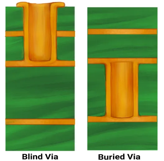
What Are Blind and Buried Vias?
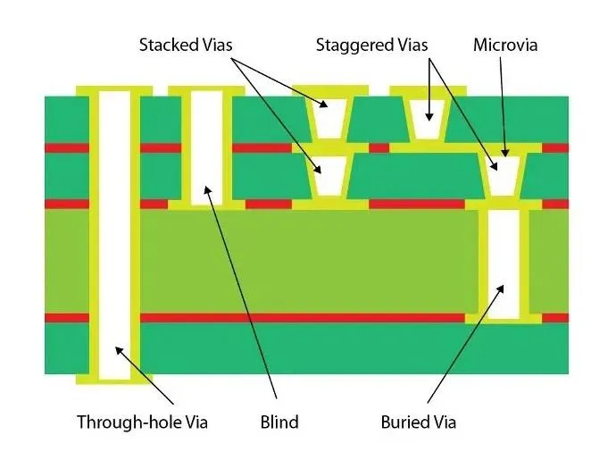
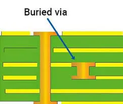
Blind vias connect an outer layer to one or more inner layers without extending through the entire board thickness. Buried vias, in contrast, link only internal layers and remain completely hidden from the surfaces. Both differ from through-hole vias, which traverse all layers and occupy routing space on every level. These advanced vias support high-density interconnect designs by freeing surface real estate for traces and components. Engineers specify them using layer pair notations, like 1-3 for a blind via from layer 1 to layer 3. Their use requires careful planning to ensure compatibility with fabrication capabilities.
The relevance of blind or buried vias grows in multilayer boards exceeding six layers, where routing congestion becomes a limiting factor. They matter for applications demanding compact form factors, such as handheld devices or server modules. By reducing via stubs, these structures also improve signal integrity at high frequencies. Fabrication costs for standard through-hole processes scale with layer count and board size, making vias that optimize these parameters valuable. In essence, they shift design trade-offs from adding layers to refining interconnections.
Technical Principles Behind Blind and Buried Vias
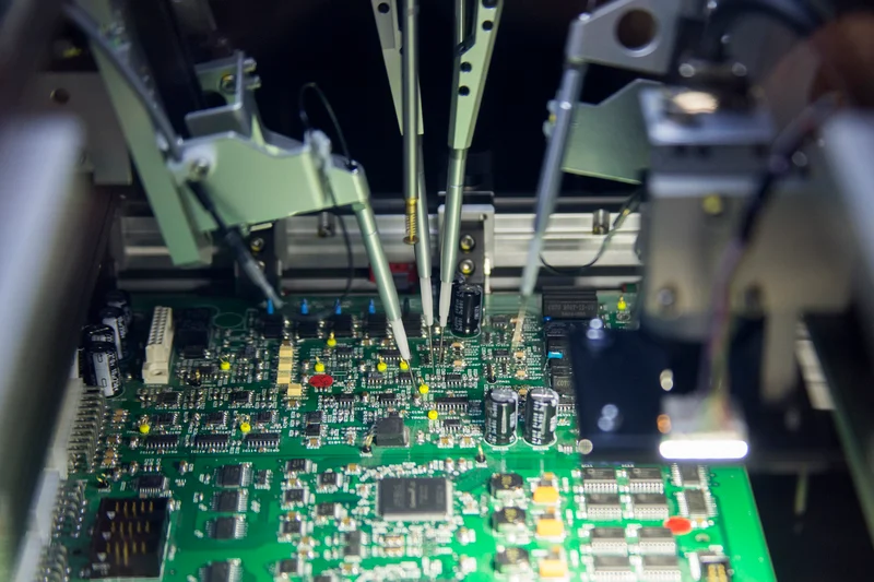
Fabrication of blind or buried vias relies on sequential lamination, where cores are built incrementally with drilling and plating between steps. Mechanical drilling creates larger vias, while laser ablation handles finer blind structures for precision. After drilling, electroless copper plating deposits a conductive barrel, followed by pattern plating and etching. This process repeats for each via structure, increasing complexity compared to all-through-hole designs. Engineers must consider aspect ratios, defined as board thickness over via diameter, to avoid plating voids or reliability issues. Compliance with IPC-6012 ensures performance specifications for rigid boards, including via geometry and plating thickness.
Buried vias demand epoxy filling post-etching to prevent resin starvation during subsequent laminations. IPC-4761 outlines via protection methods, such as Type V for buried vias, which encapsulates the hole without copper capping. This approach minimizes process steps and supports finer line spacing. Blind vias often stack or stagger to reach deeper layers, influencing thermal expansion matching between copper and dielectrics. Electrical performance benefits from shorter via lengths, reducing inductance and capacitance parasitics. These principles guide designers in selecting via types that align with signal speed and power delivery needs.
How Blind or Buried Vias Can Reduce Fabrication Costs
Strategic use of blind or buried vias addresses routing bottlenecks under dense components like BGAs, where through vias block escape routes. By limiting via penetration, designers widen breakout channels on inner layers, accommodating more traces without extra routing layers. For instance, replacing through vias with blind structures in an eight-layer stack can eliminate two dedicated routing layers, directly cutting material and lamination expenses. This layer reduction outweighs the added via fabrication steps in high-density scenarios.
Board thickness optimization represents another cost lever. High aspect ratios in thick boards with fine-pitch BGAs force larger via drills, risking clearance violations and penalties. Blind vias allow thinner stacks by connecting only necessary layers, maintaining manufacturable ratios and enabling smaller via sizes. Overall board area shrinks as surface space opens for components, further lowering copper and substrate consumption. Fabrication houses charge premiums for high layer counts or complex builds, so simplification via these vias yields net savings.
- Through-Hole: Penetration - Full board; Routing Benefit - Simple fab, but congests all layers; Cost Impact Scenario - Baseline for low density
- Blind: Penetration - Outer to inner; Routing Benefit - Frees inner routing; Cost Impact Scenario - Layer reduction under BGAs
- Buried: Penetration - Inner only; Routing Benefit - Maximizes surface space; Cost Impact Scenario - Thinner boards, high layers
Best Practices for Implementing Blind or Buried Vias
Start with stackup planning to define via pools, grouping by layer pairs to minimize lamination cycles. Use the largest viable via diameters for reliability, as smaller ones demand laser processes. Stagger stacked vias to distribute stress and avoid alignment issues during thermal cycling. Consult fabricators early for capabilities, such as sequential build limits or fill methods per IPC-4761. Optimize BGA fanouts by fanning signals outward with blind vias directly to power planes.
Via-in-pad designs enhance density but require filled and planarized structures for assembly compatibility. Simulate signal integrity to confirm stub elimination benefits. Limit via variety to reduce setup costs. Document layer designations clearly in fabrication drawings. These practices ensure cost-effective outcomes while upholding quality.
Impact on the Assembly Process
Blind or buried vias indirectly lower assembly costs by maximizing surface real estate for components. With fewer through vias piercing surfaces, pick-and-place machines navigate cleaner areas, reducing programming complexity. Under-BGA routing improves, supporting finer pitches without dog-bone escapes. Filled vias prevent solder wicking during reflow, maintaining planarity for reliable joints. This setup simplifies stencil design and inspection, as hidden vias pose no contamination risks. Overall, denser boards assemble faster with higher yields.
Conclusion
Blind or buried vias transform PCB design by enabling efficient layer utilization and density without proportional cost escalation. While their fabrication adds steps, benefits in layer and size reduction deliver net savings in targeted applications. Electrical engineers benefit from improved signal paths and compact footprints. Adhering to standards like IPC-6012 and IPC-4761 ensures reliability. Evaluate designs holistically to leverage these vias for fabrication cost optimization. Future trends in HDI will amplify their value in advanced electronics.
FAQs
Q1: When do blind or buried vias lower fabrication costs in PCB design?
A1: Blind or buried vias reduce fabrication costs primarily when they enable fewer layers or smaller board sizes in high-density layouts, such as BGA-heavy designs. By opening routing channels and eliminating unnecessary planes, material usage drops despite added lamination steps. This approach suits multilayer boards where through vias cause congestion. Always verify with fabricator capabilities for net savings.
Q2: How do blind or buried vias affect the assembly process?
A2: These vias free surface space, simplifying component placement and SMT processes by reducing via obstacles. Filled blind vias ensure flat pads for reliable soldering, minimizing defects. They support denser packing, shortening assembly cycles. Overall, they enhance yield without complicating reflow or inspection.
Q3: What standards guide blind or buried via implementation?
A3: IPC-6012 provides qualification specs for rigid boards, covering via plating and geometry. IPC-4761 details protection like Type V for buried vias, aiding sequential builds. These ensure manufacturability and performance. Compliance avoids rework costs.
Q4: Can blind or buried vias always reduce costs?
A4: No, they can increase costs in low-density designs due to more complex fabrication. Savings occur in scenarios demanding high routing efficiency, like layer optimization. Assess design density first.
References
IPC-6012E — Qualification and Performance Specification for Rigid Printed Boards. IPC, 2015
IPC-4761 — Via Protection Guidelines. IPC, 2008
IPC-A-600K — Acceptability of Printed Boards. IPC, 2020