Introduction
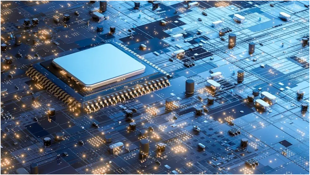
DC-DC converters form the backbone of modern power electronics, converting voltages efficiently across a wide range of applications from telecommunications to electric vehicles. As systems demand higher power density in smaller footprints, traditional thin copper traces struggle with current handling, resistive losses, and heat buildup. Thick copper PCBs address these challenges by providing robust current-carrying capacity and superior thermal performance, enabling compact designs without sacrificing efficiency. These boards feature copper layers significantly heavier than standard 1 ounce per square foot, allowing power components like inductors and transformers to integrate directly onto the PCB. This integration supports high-efficiency power converter design, where minimizing size and maximizing performance are critical. Engineers increasingly rely on thick copper PCB for DC-DC converters to meet stringent efficiency targets in space-constrained environments.
The shift toward planar transformer design further amplifies the role of thick copper, replacing bulky wire-wound components with flat, PCB-embedded windings. This approach reduces parasitic effects and improves repeatability in manufacturing. Thermal management in DC-DC converters becomes more predictable with thicker copper acting as a heat spreader, preventing hotspots that degrade component life. PCB layout for minimizing EMI also benefits, as wide traces and solid planes shield sensitive signals. Overall, thick copper PCBs unlock the potential for next-generation converters that balance compactness, efficiency, and reliability.
What Are Thick Copper PCBs and Why Do They Matter for DC-DC Converters?
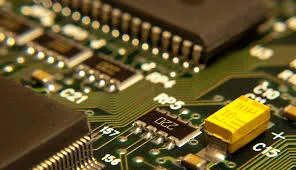
Thick copper PCBs incorporate copper foils with weights typically exceeding 1 ounce per square foot, often reaching 2 to 6 ounces or more in power applications. This increased thickness directly enhances the board's ability to carry high currents with minimal voltage drop, a key requirement for DC-DC converter power stages. Standard thin copper layers generate excessive heat under load due to higher resistance, leading to efficiency losses and thermal runaway risks. In contrast, thick copper reduces these issues, supporting high-efficiency power converter design by lowering conduction losses.
The relevance to DC-DC converters stems from the need for higher power densities in compact modules. Converters in servers, automotive systems, and renewable energy inverters must handle tens to hundreds of amps while fitting into tight spaces. Thick copper enables this by allowing wider traces and embedded passives, reducing the bill of materials and assembly complexity. Moreover, planar transformer design thrives on thick copper layers, where interleaved windings achieve tight coupling and low leakage inductance. Without thick copper, such designs would face current limitations and poor thermal dissipation, compromising overall system performance.
Engineers value thick copper for its alignment with industry demands for reliability under stress. It facilitates thermal management in DC-DC converters by spreading heat evenly across larger areas, delaying the onset of derating. This capability proves essential in environments with limited airflow or active cooling.
Technical Principles of Thick Copper in DC-DC Converter Performance
The core principle behind thick copper's effectiveness lies in fundamental electrical and thermal properties. Resistance in a conductor follows R equals rho times length over cross-sectional area, where thicker copper increases the area and proportionally reduces resistance. In DC-DC converters, this translates to lower I squared R losses, directly boosting efficiency, especially at high switching frequencies. Power stages with synchronous rectifiers and high-phase-count topologies benefit most, as current ripples demand robust conduction paths.
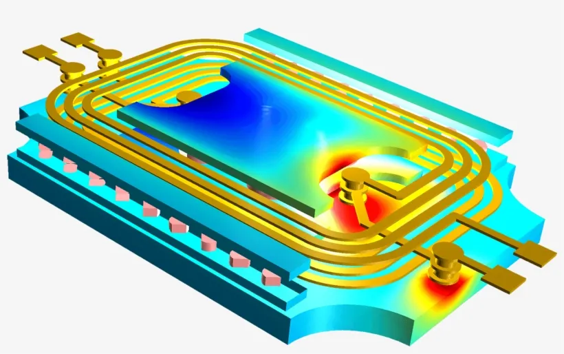
Thermal conduction follows a similar logic, with copper's high thermal conductivity around 400 W per meter-kelvin enabling rapid heat spreading. In thick copper implementations, heat from switching elements dissipates across the plane before reaching critical junctions, improving device longevity. This principle underpins thermal management in DC-DC converters, where junction temperatures must stay below thresholds for silicon or wide-bandgap devices. Engineers model these effects using finite element analysis to predict hotspots, confirming thick copper's role in uniform temperature profiles.
Planar transformer design leverages thick copper for optimal magnetic performance. Spiral or helical windings etched into multiple layers achieve high fill factors and low AC resistance, minimizing proximity and skin effects. Interlayer coupling improves with via connections, and thick copper handles the DC bias currents without saturation. This design paradigm supports isolated converters with efficiencies exceeding 95 percent in compact forms.
EMI generation in converters arises from fast dv/dt and di/dt transients, coupling into nearby circuits. Thick copper planes act as low-impedance return paths, containing fields and reducing radiated emissions. PCB layout for minimizing EMI incorporates these planes strategically, with stitching vias to maintain continuity.
Best Practices for High-Efficiency Power Converter Design with Thick Copper PCBs
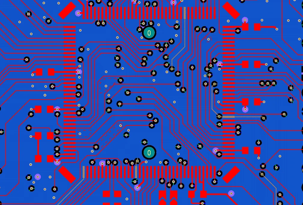
Start with layer stackup planning, prioritizing power and ground planes adjacent to signal layers for shielding. Thick copper on inner layers balances rigidity and manufacturability, while outer layers suit surface-mount components. Adhere to IPC-2221 guidelines for trace spacing and current capacity to prevent electromigration under prolonged high loads. Simulate the stackup for impedance control, ensuring signal integrity alongside power delivery.
For planar transformer design, optimize turn ratios by varying layer counts and trace widths qualitatively wider in thick copper to match current density. Place primary and secondary windings on alternating layers to minimize leakage, and use blind vias for interleaving without through-hole penetrations. This configuration enhances coupling coefficients and supports zero-voltage switching in resonant topologies.
Thermal management in DC-DC converters requires integrated strategies beyond thick copper alone. Embed thermal vias under high-power ICs, arrayed in grids to channel heat to inner planes or external heatsinks. Copper pours around inductors fill voids, promoting convection. Monitor board-level temperatures during qualification per IPC-6012 performance specs to validate designs under rated conditions.
PCB layout for minimizing EMI demands symmetry in current paths, with input capacitors close to the controller and output filters decoupled locally. Split planes carefully, avoiding splits under high di/dt traces, and route quiet signals away from switch nodes. Guard traces and ground stitching every few millimeters contain fringing fields. These practices, combined with thick copper's shielding, often meet regulatory limits without additional filters.
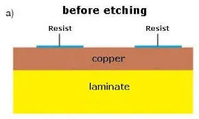
Manufacturing thick copper PCBs involves sequential lamination to control warpage, with filler materials matching CTE coefficients. Differential etching techniques ensure uniform trace profiles, preventing undercuts that raise resistance. Post-fabrication, X-ray inspection verifies via fill in high-aspect-ratio holes.
Challenges and Solutions in Thick Copper DC-DC Implementations
One common challenge is increased board stiffness from thick copper, potentially leading to via stress during thermal cycling. Mitigate this with balanced stackups and CTE-matched cores, following J-STD-001 soldering requirements for reliability. Another issue involves higher fabrication costs, offset by reduced component count and assembly steps in compact designs.
Engineers often troubleshoot EMI spikes from parasitic capacitances in planar transformers. Solutions include shielding layers and ferrite-infused dielectrics between windings. For thermal bottlenecks, hybrid cooling with embedded heat pipes complements thick copper spreading.
Conclusion
Thick copper PCBs revolutionize DC-DC converter design by enabling compact, high-efficiency solutions through superior current handling, thermal dissipation, and EMI control. Key principles like reduced resistance and enhanced conduction directly support planar transformer design and overall power density goals. These advantages make heavy-copper PCB application solutions especially valuable in modern power electronics, including industrial power supplies, automotive converters, renewable energy systems, telecom infrastructure, and high-current battery management platforms. Best practices in layout, stackup, and manufacturing ensure reliable performance aligned with industry standards. As power electronics evolve, thick copper remains indispensable for engineers pushing efficiency boundaries in thermal management in DC-DC converters. Adopting these boards positions designs for future scalability and robustness.
FAQs
Q1: What are the main benefits of using thick copper PCB for DC-DC converters?
A1: Thick copper provides high current capacity with low resistance, reducing conduction losses for high-efficiency power converter design. It excels in thermal management by spreading heat effectively, allowing compact layouts without excessive temperatures. Planar transformer integration becomes feasible, minimizing size compared to wire-wound alternatives. Overall, it supports reliable operation under high loads with proper PCB layout for minimizing EMI.
Q2: How does planar transformer design benefit from thick copper PCBs?
A2: Thick copper enables wide, low-resistance windings in multilayer stackups, improving DC handling and reducing AC losses from skin effects. Tight interlayer coupling via vias achieves high efficiency in isolated converters. The flat profile aids compact assembly, and inherent shielding helps PCB layout for minimizing EMI. This design suits high-frequency operation where traditional transformers falter.
Q3: What strategies improve thermal management in DC-DC converters with thick copper PCBs?
A3: Leverage thick copper planes for heat spreading, augmented by via arrays under hotspots to inner layers. Balance stackups to minimize warpage and ensure uniform dissipation. Local decoupling and airflow paths prevent localized overheating. These approaches maintain junction temperatures within limits, enhancing longevity in high-efficiency power converter design.
Q4: How can PCB layout minimize EMI in thick copper DC-DC converters?
A4: Use solid ground planes with stitching vias for low-impedance returns, routing high di/dt paths over continuous copper. Symmetrize current loops and shield signals with guard traces. Place filters near sources to contain noise. Thick copper enhances this by providing effective shielding, meeting emission standards efficiently.
References
IPC-2221B — Generic Standard on Printed Board Design. IPC, 2012
IPC-6012DS — Qualification and Performance Specification for Rigid Printed Boards. IPC, 2015
J-STD-001G — Requirements for Soldered Electrical and Electronic Assemblies. IPC, 2011