Introduction
High-density interconnect (HDI) PCBs enable compact electronics with superior routing density and signal performance, critical for applications like smartphones and medical devices. Sequential lamination plays a pivotal role in fabricating these boards by allowing the integration of blind vias sequential lamination and buried vias HDI PCB structures. Unlike standard multilayer processes, this method builds the board through multiple lamination cycles, creating precise interconnections without through-vias spanning the entire stack. Electric engineers must understand these techniques to optimize HDI PCB design rules and ensure manufacturability. This guide explores the principles, processes, and best practices for microvia PCB fabrication using sequential lamination. By mastering via in pad sequential lamination, designers can achieve higher reliability and density in their layouts.
What Is Sequential Lamination and Why It Matters in HDI PCBs
Sequential lamination involves constructing HDI PCBs by laminating subsets of layers in successive cycles, rather than bonding all layers at once. This approach is essential for incorporating blind and buried vias, which connect specific layers without penetrating the full board thickness. In standard multilayers, through-vias create stubs that degrade signal integrity, but sequential lamination eliminates these by enabling targeted via structures. For electric engineers, this method supports advanced HDI classes, such as 1-n-1 or stacked microvias, directly impacting board size reduction and performance. Factory processes rely on it for high layer counts, where alignment precision determines yield. Ultimately, sequential lamination aligns with IPC-2226A requirements for HDI design, ensuring robust interconnections in demanding environments.
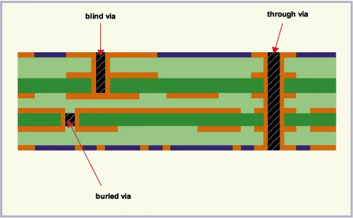
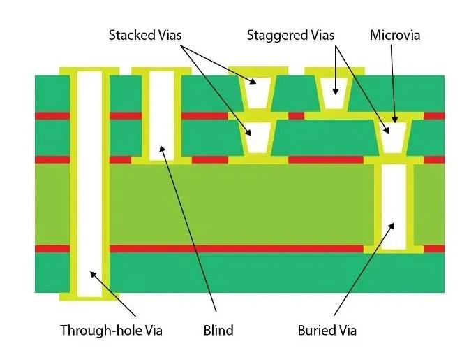
Blind vias extend from an outer layer to one or more inner layers, remaining invisible from the opposite side. Buried vias link inner layers exclusively, fully enclosed within the stackup. These structures, formed during sequential build-up, allow finer pitch routing and shorter signal paths. In HDI contexts, they often pair with microvias, laser-drilled for diameters under 150 microns. Engineers benefit from reduced inductance and capacitance compared to through-vias. Proper implementation via sequential lamination prevents issues like via breakout failures during assembly.
Technical Principles of Sequential Lamination for Blind and Buried Vias
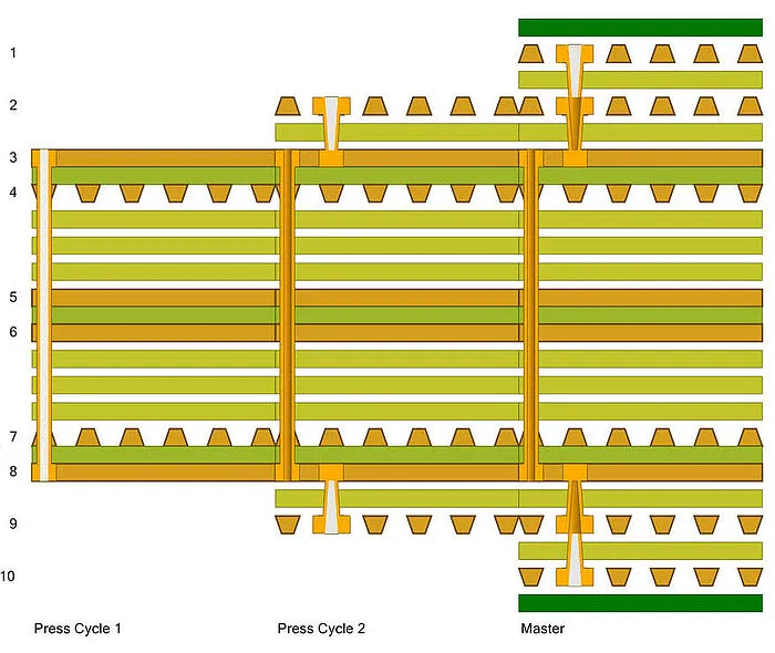
The core principle of sequential lamination lies in iterative sub-stack assembly, where each cycle adds layers, drills vias, and plates them before the next bonding. Factories begin with a central core of two or more layers, etching circuits and drilling initial through-holes if needed for buried vias. Prepreg sheets bond this core to outer foils, forming the first sub-composite. Blind vias are then drilled from the new outer layer into the core, electroplated, and imaged for circuitry. This cycle repeats, registering each sub-stack precisely to maintain layer alignment.
For buried vias HDI PCB fabrication, inner cores receive plated through-holes before outer build-ups, ensuring connections between non-adjacent internal layers. Laser drilling follows for microvias in subsequent steps, targeting dielectric precisely without damaging underlying copper. Plating fills these vias, often with copper electroplating to form reliable barrels. Sequential lamination supports stacked configurations, where microvias align atop buried vias, or staggered ones for stress distribution. Each lamination cures resins under controlled heat and pressure, solidifying bonds while minimizing voids.
Alignment relies on tooling pins and fiducials, critical as tolerances tighten to microns in HDI. Warpage arises from coefficient of thermal expansion mismatches between copper and dielectrics during cycles, potentially lifting pads or cracking resins. Factories mitigate this through symmetric stackups and material selection with matched properties. IPC-6016 outlines qualification tests for these structures, verifying via integrity post-lamination.
Microvia PCB Fabrication in Sequential Lamination
Microvia PCB fabrication integrates seamlessly with sequential lamination, using UV or CO2 lasers to ablate dielectrics for blind microvias. After each lamination, engineers specify via locations connecting to capture pads on prior layers. Sequential desmear removes residue, followed by sequential chemical and electrolytic plating to deposit copper. Via in pad sequential lamination allows microvias to land directly on components or fine traces, maximizing density. Factories control aspect ratios to ensure uniform plating, avoiding voids or thinning.
In HDI stacks, microvias can stack up to three levels per IPC guidelines, with each level added in a dedicated lamination cycle. Buried microvias form similarly within inner sub-stacks. Post-plating, outer layers receive imaging and etching, completing the cycle. This build-up enables net densities exceeding traditional methods, vital for BGA fanouts.
Challenges include resin smear migration during drilling, addressed by plasma cleaning. Thermal stresses from multiple cycles demand high-Tg dielectrics to prevent delamination. Final X-ray inspection confirms via fill and alignment before outer finishes.
HDI PCB Design Rules for Sequential Lamination
HDI PCB design rules dictate stackup planning to minimize lamination cycles, typically limiting to two or three for cost efficiency. Blind vias sequential lamination requires defining via spans, such as L1-L2 or L1-L4, with capture pads oversized for registration tolerances. Buried vias need pre-planned in core stackups, avoiding conflicts with surface routing. Via in pad designs mandate flat copper filling to prevent solder wicking issues during assembly.
Engineers must balance via density with drill capabilities, favoring staggered over stacked microvias for reliability under thermal cycling. IPC-2226A provides guidelines for pad sizes, annular rings, and breakout routing to ensure manufacturability. Stackup symmetry counters warpage, with core thickness influencing overall bow. Signal integrity rules limit stub lengths inherent in blind structures.
Fabrication feedback loops refine rules, such as minimum dielectric thickness between vias. Designers simulate CTE effects to predict stress zones around buried vias.
Best Practices and Practical Solutions in Factory Production
Select low-CTE, high-Tg prepregs for sequential cycles to reduce Z-axis expansion and warpage. Factories use carrier films on outer foils for flatness during pressing. Precise tooling holes and optical alignment systems maintain sub-micron registration across cycles. For via in pad sequential lamination, electroplating parameters ensure void-free fills compatible with reflow.
Monitor lamination parameters like pressure and ramp rates to avoid voids, verifying with C-scan ultrasound. Post-cycle black oxide or alternative bonding treatments enhance adhesion. Scale artwork for shrinkage compensation, especially in asymmetric builds. Electrical testing after each major cycle catches opens early.
Troubleshooting warpage involves back-drilling stubs or adding constraint layers. For high-reliability HDI, qualify per IPC-6016 with thermal shock and reliability tests.
Challenges and Mitigation Strategies
Multiple lamination cycles amplify risks like delamination from resin flow inconsistencies into vias. Factories address this by optimizing prepreg resin content and flow characteristics. Alignment drift accumulates, mitigated by redundant fiducials and automated drilling. Plating uniformity challenges arise in deep blind vias, resolved via pulse plating techniques.
Warpage testing post-lamination guides adjustments, using dial gauges for bow measurement. Stress concentrations around stacked vias on buried structures demand larger landing pads. Material selection prioritizes low-loss tangents for high-speed signals.
Conclusion
Sequential lamination unlocks the full potential of blind and buried vias in HDI PCBs, enabling compact, high-performance designs. Electric engineers gain from structured processes that integrate microvia PCB fabrication with precise HDI PCB design rules. Factory insights emphasize alignment, material choices, and cycle optimization for yield. Adhering to standards like IPC-2226A ensures reliability. Mastering via in pad sequential lamination positions teams for next-generation electronics.
FAQs
Q1: What is blind vias sequential lamination in HDI PCBs?
A1: Blind vias sequential lamination builds connections from outer layers to inner ones through iterative lamination cycles. Factories create sub-stacks, drill targeted vias, plate them, and bond additional layers. This method supports microvias without full through-holes, improving density. Design stackups to limit cycles for cost control, aligning with IPC guidelines for pad sizing.
Q2: How does buried vias HDI PCB fabrication differ from standard multilayers?
A2: Buried vias HDI PCB fabrication uses sequential lamination to connect inner layers exclusively, formed in core sub-stacks before outer build-ups. Drilling and plating occur pre-lamination for these vias, avoiding surface exposure. This reduces inductance versus through-vias. Engineers plan cores symmetrically to manage warpage during multiple presses.
Q3: What are key HDI PCB design rules for microvia PCB fabrication?
A3: HDI PCB design rules for microvia PCB fabrication specify via spans, capture pads, and dielectric thicknesses per sequential lamination needs. Favor staggered microvias over stacked for stress relief. Ensure annular rings accommodate registration tolerances. Stackup planning minimizes cycles while maximizing routing density.
Q4: When is via in pad sequential lamination recommended?
A4: Via in pad sequential lamination suits high-density BGA escapes and fine-pitch components in HDI boards. It allows vias to fill with copper, enabling direct soldering. Sequential cycles ensure plating integrity. Use for space-constrained designs, verifying fill with cross-sections.
References
IPC-2226A — Sectional Design Standard for High Density Interconnect (HDI) Printed Boards. IPC, 2017
IPC-6016 — Qualification and Performance Specification for High Density Interconnect (HDI) Layers or Boards. IPC, 1999
IPC-6012E — Qualification and Performance Specification for Rigid Printed Boards. IPC, 2017


