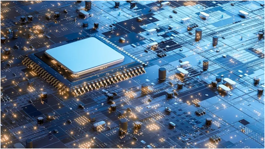
HDI PCB Manufacturing enables the production of ultra-compact, high-performance circuit boards that power modern electronics. From smartphones and medical wearables to 5G modules and autonomous vehicles, this specialized manufacturing discipline delivers higher component density, shorter signal paths, and superior electrical performance compared with conventional PCB fabrication.
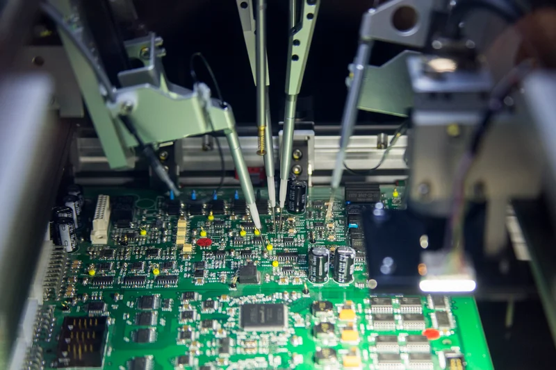
Manufacturers and engineers rely on HDI PCB Manufacturing to meet strict miniaturization demands while maintaining reliability under thermal cycling, high-frequency operation, and mechanical stress. The process integrates precision laser drilling, sequential lamination, advanced etching, and rigorous quality control to produce boards with microvias as small as 0.075 mm and trace widths under 50 µm.
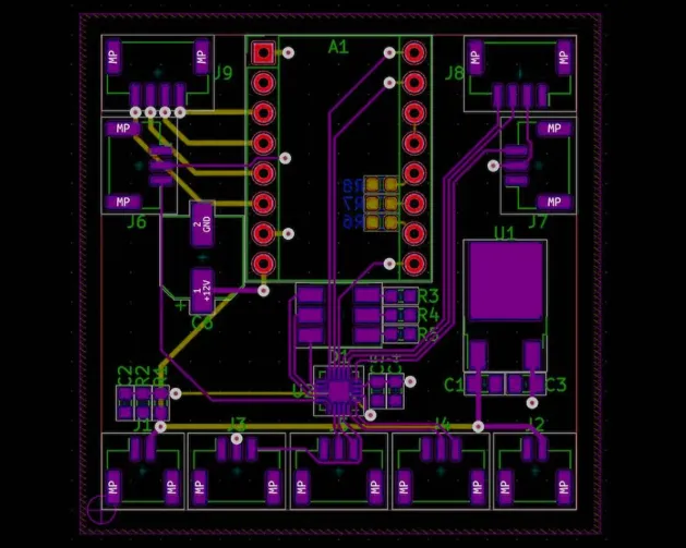
The Complete Step-by-Step HDI PCB Manufacturing Process Flow from Substrate to Final Inspection
The manufacturing workflow begins with material selection and ends with final inspection:
- Substrate Preparation – Choose high-Tg laminates or low-loss dielectrics with precise thickness tolerance (±10%).
- Laser Drilling of Microvias – Create 0.075–0.15 mm holes with ±25 µm accuracy using UV or CO₂ lasers.
- Desmear and Electroless Copper Deposition – Ensure void-free plating inside microvias with controlled plating thickness of 15–25 µm.
- Pattern Plating and Etching – Form fine traces using semi-additive or modified semi-additive processes.
- Sequential Lamination – Build additional layers with controlled pressure, temperature, and vacuum to prevent delamination.
- Via Filling and Planarization – Use conductive or non-conductive epoxies followed by copper capping and surface leveling.
- Surface Finish and Final Inspection – Apply ENIG, OSP, or immersion silver and verify all features.
Each step requires tighter process windows than standard PCB manufacturing to prevent defects such as plating voids, delamination, or impedance drift.
Cutting-Edge Technologies Transforming HDI PCB Production
Advanced PCB manufacturing innovations in high-density interconnect HDI technology drive the next generation of fabrication. Key breakthroughs include laser ablation microvia formation, electroplated copper via filling, plasma cleaning for superior adhesion, vacuum-assisted via filling, and AI-driven real-time process monitoring.
These innovations enable finer lines under 30 µm, higher via densities, and improved electrochemical migration resistance. Manufacturers gain reduced board footprint, enhanced signal integrity at higher speeds, better thermal dissipation, and greater reliability under extreme thermal stresses.
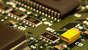
Precision Etching Methods for Ultra-Fine HDI Circuitry
Advanced PCB etching techniques for high-density interconnect HDI boards are essential for achieving the fine-line resolution required in modern HDI production. The semi-additive process (mSAP) combined with laser direct imaging (LDI) and plasma reactive ion etching delivers trace widths and spaces under 50 µm with excellent edge definition.
These techniques minimize undercutting, reduce copper thickness variation, and support microvia etching precision. Best practices include precise etch factor control, advanced resist chemistry, and in-line metrology to maintain yield above 98% on high-density panels.
Choosing Optimal Materials for High-Frequency HDI Boards
HDI PCB materials selection for high-frequency applications directly determines signal integrity and thermal performance. Low-loss laminates with low dielectric constant (Dk) and low dissipation factor (Df) minimize insertion loss at 5G and millimeter-wave frequencies.
Engineers select materials compliant with IPC-4103 that offer stable Dk/Df over temperature, high glass transition temperature (Tg) for thermal stability, controlled coefficient of thermal expansion (CTE), and excellent laser-drilling compatibility. These properties prevent signal degradation, layer mismatch, and via defects during high-frequency operation.
Moving Past Standard FR-4 to High-Performance Substrates
Beyond FR-4 selecting the right materials for high-performance HDI PCBs opens the door to superior alternatives. High-Tg modified epoxy, polyimide resins, low-loss polyphenylene ether or hydrocarbon-based dielectrics, and ceramic-filled laminates deliver improved thermal stability, reduced signal loss, enhanced heat dissipation, and better mechanical integrity.
These advanced substrates support higher operating frequencies, greater power densities, and harsher environmental conditions while maintaining compatibility with microvia formation and sequential lamination processes.
Rigorous Quality Assurance Protocols for Reliable HDI Boards
HDI PCB quality control ensuring reliability and performance is non-negotiable for high-density boards. Rigorous material verification against IPC-4101 and IPC-4103 standards, dimensional and structural inspection, electrical performance testing, automated optical inspection (AOI), X-ray analysis for hidden via defects, and thermal cycling or HAST testing form the backbone of a robust quality system.
Best practices include 100% via fill inspection, impedance coupon verification, and statistical process control. These measures guarantee boards meet IPC-6012E Class 3 requirements and pass 1,000+ thermal cycles with minimal resistance drift.
Common HDI Production Issues and How to Resolve Them
Troubleshooting common HDI PCB problems a practical guide helps manufacturers quickly resolve issues. The most frequent defects include microvia plating failures, signal integrity problems, delamination from thermal stress, solder joint defects, and board warpage.
Solutions involve optimizing microvia aspect ratios, selecting low-CTE materials, implementing precise etch and lamination parameters, controlling reflow profiles, and applying strict process monitoring. Early identification through AOI, X-ray, and electrical testing prevents costly scrap and field failures.
Real-World Case Study: 12-Layer HDI Board for 5G Small-Cell Module
A leading 5G equipment manufacturer needed a compact 12-layer HDI PCB for a millimeter-wave small-cell module. The board required 0.3 mm pitch BGAs, 25 µm trace/space, and 0.1 mm laser-drilled microvias while operating at 28 GHz.
Using advanced PCB manufacturing innovations in high-density interconnect HDI technology, the team selected a low-loss hydrocarbon laminate (Dk = 3.2, Df = 0.002) and applied mSAP etching. They implemented vacuum-assisted copper via filling and strict HAST testing.
Result: 99.2% first-pass yield, 40% size reduction versus previous design, and stable insertion loss below 0.8 dB/inch at 28 GHz. The project completed in 8 weeks and passed 2,000 thermal cycles with zero field failures.
Emerging Future Trends Shaping HDI PCB Manufacturing
HDI PCB Manufacturing is evolving rapidly toward even finer features and smarter production.
- AI and machine learning will optimize real-time process control, predicting defects before they occur and pushing yields above 99.5%.
- Sub-20 µm line/space via next-generation mSAP and SAP processes will become mainstream for AI accelerators and high-speed computing.
- Sustainable and halogen-free low-loss materials will dominate as environmental regulations tighten.
- Hybrid integration with fan-out wafer-level packaging and embedded components will blur the line between PCB and semiconductor packaging.
- Additive manufacturing (3D-printed conductors and dielectrics) may eventually reduce waste and enable fully customized stack-ups.
These trends will further shrink board sizes while raising reliability standards for 6G, autonomous driving, and medical implant applications.
Best Practices, Industry Standards, and Learning Resources
To achieve consistent high yields and long-term reliability in HDI PCB Manufacturing, follow these core best practices at every stage of production:
- Conduct early design-for-manufacturability (DFM) reviews with your fabricator to align microvia aspect ratios, trace clearances, and stack-up symmetry before artwork release.
- Maintain cleanroom environments (Class 100 or better) and use low-residue chemistry during etching and plating to minimize contamination that causes electrochemical migration.
- Implement 100% via-fill inspection using X-ray or cross-section analysis and verify copper thickness uniformity within ±10% on every production panel.
- Apply statistical process control (SPC) on critical parameters such as laser-drill accuracy, lamination pressure, and etch factor to keep process capability (Cpk) above 1.33.
- Select materials only after reviewing supplier data sheets against IPC-4101 and IPC-4103, and qualify new laminates with test vehicles before full-scale production.
- Document every process parameter (temperature profiles, chemical concentrations, plating times) for full traceability and continuous improvement.
Adhere to the following industry standards as mandatory references:
- IPC-2226 for HDI design rules and microvia specifications
- IPC-6012E Class 3 for performance and reliability requirements
- IPC-A-600K for acceptance criteria of printed boards
- IPC-4101 and IPC-4103 for base-material qualifications
To deepen your expertise, study these standards directly from the IPC website, attend manufacturer technical webinars on mSAP and laser drilling, and review detailed material datasheets and application notes from laminate suppliers. Join specialized electronics manufacturing forums and participate in hands-on training courses focused on HDI processes. Download this complete guide and apply one new best practice on your next prototype run to build practical mastery quickly.
Conclusion
HDI PCB Manufacturing represents the pinnacle of precision electronics fabrication. By mastering the detailed process flow, adopting cutting-edge innovations and etching techniques, selecting high-performance materials, implementing rigorous quality control, and applying proven troubleshooting methods, manufacturers can consistently deliver reliable, high-density boards. Real-world case studies confirm that these practices yield dramatic size reductions and superior high-frequency performance, while emerging trends promise even greater capabilities for future applications. Whether you are scaling production or refining prototypes, following the comprehensive strategies outlined in this guide positions you for success in the evolving landscape of HDI technology.
FAQs
Q1: How do advanced etching techniques improve HDI yield?
A1: Semi-additive and laser direct imaging processes deliver finer lines, sharper edges, and tighter tolerances, reducing shorts and opens by up to 40%.
Q2: Which materials should I choose for high-frequency HDI boards?
A2: Select low-loss laminates with Dk < 3.5 and Df < 0.003, high Tg (> 170 °C), and excellent laser-drilling compatibility.
Q3: What is the most critical step in HDI PCB Manufacturing?
A3: Microvia formation and reliable copper plating are the most critical, because any void or crack leads to immediate electrical failure.
Q4: How can I troubleshoot microvia plating failures?
A4: Optimize aspect ratio, improve desmear process, use vacuum-assisted filling, and verify plating thickness with cross-section analysis.