Introduction
High-density interconnect (HDI) technology represents a cornerstone of advanced PCB manufacturing, enabling the creation of compact, high-performance printed circuit boards essential for modern electronics. As electronic devices continue to shrink while demanding greater functionality, HDI PCB manufacturing has evolved to incorporate microvias, blind vias, and buried vias, allowing for denser component placement and improved signal integrity. This innovation addresses the limitations of conventional PCBs by supporting finer line widths and spaces, which are critical for applications in telecommunications, medical devices, and consumer electronics. Factory processes for HDI PCBs emphasize sequential lamination and precise via formation to achieve reliability under demanding conditions. Engineers benefit from these advancements through reduced board size and enhanced electrical performance, making HDI a preferred choice in high-volume production environments.
What Is High-Density Interconnect (HDI) Technology and Why It Matters
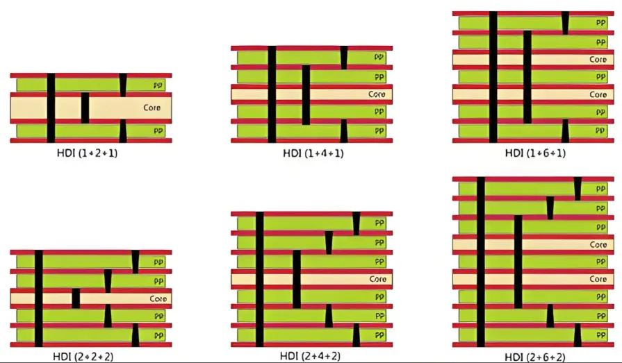
High-density interconnect PCB technology refers to multilayer boards that utilize microvias, stacked or staggered vias, and fine-feature interconnects to achieve higher wiring density per unit area compared to standard rigid PCBs. Microvia PCB manufacturing involves laser-drilled vias with small diameters, typically connecting adjacent layers without penetrating the entire board thickness. This approach supports build-up structures classified as 1+n+1, 2+n+2, or more complex configurations, where "n" denotes the number of core layers. The relevance of HDI lies in its ability to meet the miniaturization demands of electric engineers designing for space-constrained products like smartphones and wearables. In manufacturing, HDI reduces overall board footprint by up to significant margins while maintaining or improving thermal and electrical properties. Adherence to established standards ensures these boards perform reliably in high-frequency applications.
HDI technology matters profoundly in advanced PCB technology because it facilitates the integration of more components in smaller areas, directly impacting product portability and efficiency. Conventional through-hole vias waste valuable real estate and introduce inductance, whereas HDI's blind and buried vias optimize routing paths for better signal speeds. Factories producing HDI PCBs prioritize process control to mitigate risks like via failures during thermal cycling. This technology also supports the transition to finer pitches for ball grid arrays and chip-scale packages, aligning with industry trends toward system-in-package designs. For electric engineers, mastering HDI PCB manufacturing unlocks opportunities in automotive electronics and IoT devices, where density directly correlates with performance gains.
Technical Principles of HDI PCB Manufacturing
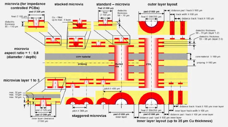
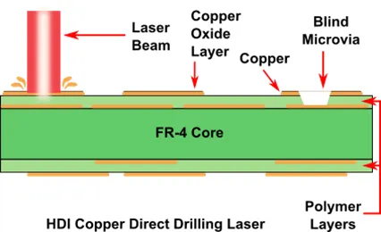
The core principle of HDI PCB manufacturing revolves around sequential lamination, a build-up process where thin dielectric layers and copper foils are added incrementally around a central core. Laser ablation forms microvias by vaporizing dielectric material with ultraviolet or CO2 lasers, creating precise apertures filled subsequently with electroplated copper for electrical connectivity. This method contrasts with mechanical drilling used for larger vias, offering superior accuracy for features under 150 microns in diameter. Factories control aspect ratios tightly to prevent plating voids, ensuring uniform copper deposition across via walls. Material selection plays a key role, with low-loss dielectrics and resin-coated copper foils enhancing high-speed signal propagation.
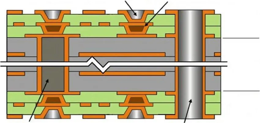
In microvia PCB manufacturing, via reliability stems from proper fill methods, such as conductive or non-conductive pastes for stacked configurations, followed by lamination cycles that cure resins without inducing stress cracks. Staggered microvias distribute mechanical loads, reducing warpage during reflow soldering, while filled vias enable via-in-pad designs for maximum density. Advanced processes incorporate plasma cleaning to improve adhesion before plating, minimizing defects like dog-boning where copper thickens at via ends. These principles align with IPC-2226 guidelines for HDI structures, dictating minimum clearances and land sizes to prevent shorts. Electrical testing verifies continuity and impedance post-fabrication, confirming the integrity of high-density interconnects.
Innovations in advanced PCB technology have refined these principles through vacuum-assisted via filling and finer laser drilling resolutions, enabling sub-50-micron vias in production. Sequential build-up allows for embedded components within layers, further densifying interconnects while managing heat dissipation via metal-filled vias. Factory-driven insights emphasize cycle time optimization, balancing throughput with quality through automated optical inspection at each lamination step. Thermal management integrates with HDI by using low-CTE materials to match component expansions.
HDI PCB Design Rules and Manufacturing Best Practices
HDI PCB design rules, as outlined in industry standards like IPC-2226, specify parameters for microvia capture and target pads, line widths, and spaces to ensure manufacturability and reliability. Engineers must account for fabrication tolerances, setting minimum trace widths around 40 microns for high-end builds while verifying stackup symmetry to control warpage. Optimal layer pairing minimizes via stubs, preserving signal integrity in high-speed designs. Factories recommend teardrops at via-to-trace junctions to reduce stress concentrations during assembly.
Optimizing HDI PCB involves strategic stackup planning, alternating signal and plane layers to control impedance and crosstalk. Use of blind vias from outer layers to inner cores reduces inductance compared to full through-vias. Best practices include simulating via transitions for resonance avoidance and selecting build-up dielectrics with matching DK values for uniform fields. In production, sequential lamination cycles incorporate controlled ramp rates to prevent delamination.
Practical solutions for microvia PCB manufacturing focus on yield enhancement through process windows defined by design rules. Pre-lamination desmear removes drill residue, ensuring plating uniformity, while post-plating planarization maintains flatness for subsequent imaging. For complex 2+n+2 structures, intermediate inspections detect misalignment early. Engineers benefit from collaborating with fabricators on DFM reviews to refine rules for specific capabilities.
Innovations Driving HDI PCB Advancements
Recent innovations in HDI PCB manufacturing include the adoption of filled microvias with conductive epoxies, enabling stacked and staggered configurations without reliability trade-offs. Laser direct imaging for photoresists achieves finer lines under 30 microns, pushing the boundaries of advanced PCB technology. Factories integrate AI-driven process monitoring to predict defects, optimizing parameters like etch rates in real-time. These developments support higher layer counts, up to 20 or more, for 5G and AI hardware.
Sustainability enters HDI through lead-free plating baths and recyclable resins, aligning with ISO 9001 quality frameworks. Enhanced copper electroplating yields smoother via walls, reducing skin effect losses at frequencies above 10 GHz. Microvia reliability improves via electrochemical migration resistance testing per IPC-6012 specifications. Factory insights highlight hybrid HDI with embedded passives, streamlining assembly while densifying boards.
Conclusion
Innovations in high-density interconnect (HDI) technology have transformed advanced PCB manufacturing, delivering boards with unprecedented density and performance for electric engineers. From laser microvia formation to sequential lamination, these processes ensure reliable interconnects under thermal and mechanical stresses. Adhering to HDI PCB design rules optimizes layouts for signal integrity and manufacturability. As demands for miniaturization grow, factories continue refining techniques like via filling and fine-line imaging. Engineers can leverage these advancements to create efficient, compact designs, supported by standard-aligned practices.
FAQs
Q1: What are the key steps in HDI PCB manufacturing?
A1: HDI PCB manufacturing begins with core preparation, followed by sequential lamination where dielectric layers and copper foils are added. Laser drilling creates microvias, which are desmeared, plated, and inspected. Outer layers are imaged, etched, and finished with surface treatments. This factory-driven process ensures high-density interconnects meet performance needs, with quality checks at each stage aligning to standards like IPC-2226.
Q2: How do HDI PCB design rules impact microvia PCB manufacturing?
A2: HDI PCB design rules define pad sizes, clearances, and via aspects to prevent defects during fabrication. Proper rules allow reliable laser drilling and plating, optimizing HDI PCB for density. Engineers must consider fabricator capabilities to avoid yield losses from overly aggressive features. Standards guide these rules for consistent high-density interconnect performance.
Q3: What best practices optimize HDI PCB signal integrity?
A3: Optimizing HDI PCB starts with impedance-controlled stackups using low-loss materials. Route high-speed signals between planes, minimizing via stubs with blind structures. Ground stitching vias reduce crosstalk in high-density interconnect layouts. Factory validation through TDR testing confirms integrity post-manufacture.
Q4: Why is sequential lamination critical in advanced PCB technology for HDI?
A4: Sequential lamination builds HDI layers incrementally, enabling precise microvia placement without core distortion. It supports complex structures like 2+n+2 for maximum density. Controlled curing prevents warpage, vital for assembly yield. This process defines advanced PCB technology reliability in production.
References
IPC-2226 — Sectional Design Standard for High Density Interconnects. IPC.
IPC-6012E — Qualification and Performance Specification for Rigid Printed Boards. IPC, 2017.
ISO 9001:2015 — Quality Management Systems. ISO, 2015.