Introduction
High Density Interconnect (HDI) Printed Circuit Boards (PCBs) are integral to modern electronics, enabling compact designs with enhanced functionality in devices like smartphones, medical equipment, and automotive systems. As the complexity of HDI PCBs increases with finer lines, smaller vias, and multiple layers, maintaining quality becomes a critical challenge for electrical engineers. Effective HDI PCB quality control methods ensure reliability, performance, and compliance with stringent industry standards. This article explores the inspection criteria, testing techniques, and best practices for achieving consistent quality in HDI PCB production. From material selection to final testing, understanding these processes is essential for engineers aiming to deliver robust and high performing circuit boards in demanding applications.
Why HDI PCB Quality Control Depends on Effective Testing and Inspection
HDI PCBs are characterized by their high wiring density, achieved through microvias, fine pitch traces, and multiple stacked layers. These boards support advanced electronic designs by reducing size and weight while increasing signal integrity and speed. However, their intricate structure makes them prone to defects like microvia failures, trace discontinuities, and layer misalignment. Poor quality can lead to signal loss, thermal issues, or complete system failure, impacting product reliability and safety.
Quality control in HDI PCB manufacturing process is vital to detect and prevent such issues early. It ensures that boards meet performance specifications and adhere to industry standards. For electrical engineers, rigorous HDI PCB inspection criteria and testing methods are non negotiable to guarantee functionality in high stakes environments such as aerospace or medical fields, where failure is not an option.
Core Quality Control Principles Behind Reliable HDI Testing
Quality control for HDI PCBs involves a systematic approach to monitor every stage of production, from design validation to final assembly. The primary focus areas include material integrity, dimensional accuracy, and electrical performance. Below are the key principles guiding HDI PCB quality control methods.
Material Selection and Verification
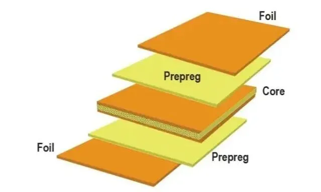
The foundation of HDI PCB reliability lies in selecting appropriate materials. Base laminates, copper foils, and dielectric layers must withstand thermal and mechanical stresses during operation. Quality control starts with verifying material properties against recognized IPC standards such as IPC 4101, which outlines specifications for laminate materials used in PCBs. Testing for thermal stability, moisture absorption, and dielectric constant ensures that materials will perform under specified conditions.
Dimensional and Structural Integrity
HDI PCBs often feature microvias with diameters below 150 micrometers and trace widths under 100 micrometers. Precision in drilling, etching, and lamination is crucial to maintain structural integrity. Inspection criteria based on IPC A 600K, which defines acceptability standards for printed boards, help engineers evaluate aspects like via alignment, layer registration, and surface finish. Deviations in these parameters can cause open circuits or shorts, undermining board performance.
Electrical Performance and Signal Integrity
Electrical testing focuses on verifying continuity, insulation resistance, and impedance control, especially critical for high speed signals in HDI designs. Standards like IPC 9252 provide guidelines for electrical test requirements, ensuring that boards meet performance benchmarks. Signal integrity issues, such as crosstalk or reflection, often stem from inconsistent trace geometry or dielectric properties, making electrical testing a cornerstone of quality control.

HDI Inspection Criteria for Microvias, Dimensions, and Layer Registration
Inspection criteria for HDI PCBs are derived from widely accepted industry standards to ensure consistency and reliability. These criteria cover visual, dimensional, and functional aspects of the board. Below are the primary categories of inspection for HDI PCBs.
Visual Inspection Standards
Visual inspection, guided by IPC A 600K, assesses surface defects, solder mask coverage, and marking clarity. Engineers look for issues like scratches, voids in plating, or incomplete solder mask application. For HDI PCBs, special attention is given to microvia formation and surface flatness, as even minor flaws can affect assembly and performance.
Dimensional Inspection
Dimensional checks verify the accuracy of features like via sizes, trace widths, and board thickness. Tools such as optical comparators and coordinate measuring machines are used to ensure compliance with design specifications. IPC 6012E, which specifies performance requirements for rigid PCBs, provides detailed acceptance criteria for these measurements, ensuring structural reliability.
Microvia and Layer Registration
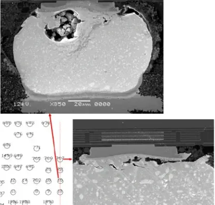
Microvias and layer alignment are critical in HDI designs due to their stacked structure. Inspection often involves cross sectioning and microscopic analysis to check via integrity and interlayer connections. Misalignment or incomplete via filling can lead to reliability issues, making adherence to IPC 2226 guidelines for HDI design and manufacturing essential.

Automated Solutions for HDI PCB Inspection and Defect Detection
As HDI PCB feature sizes continue to decrease, automated inspection systems become increasingly useful for maintaining consistent production quality. Automated optical inspection (AOI) can evaluate fine traces, solder mask features, surface defects, and other visible characteristics at high production volumes. X-ray inspection can complement AOI by examining internal structures such as buried vias, microvias, and dense interconnect regions that cannot be evaluated optically.
Automated solutions for HDI PCB inspection can also improve process consistency by generating repeatable inspection data. When inspection results are integrated with manufacturing process monitoring, engineers can identify recurring defects, track process trends, and adjust drilling, etching, lamination, or plating parameters before defects become widespread.
HDI PCB Testing Methods for Electrical and Structural Verification
Testing is a fundamental component of HDI PCB quality control, focusing on identifying defects that inspections might miss. These methods validate both mechanical and electrical properties, ensuring boards meet operational demands. Below are key HDI PCB testing approaches.
Automated Optical Inspection (AOI)
AOI systems use high resolution cameras to detect surface defects like missing traces or solder mask irregularities. This non contact method is efficient for high volume production, allowing engineers to identify issues early in the manufacturing process. It complements manual visual checks by providing consistent and repeatable results.
X Ray Inspection
X ray imaging is indispensable for inspecting internal structures of HDI PCBs, particularly microvias and buried layers. It reveals defects like voids, cracks, or incomplete via filling that are invisible to the naked eye. This method ensures compliance with structural integrity standards outlined in IPC 6012E.
Electrical Testing
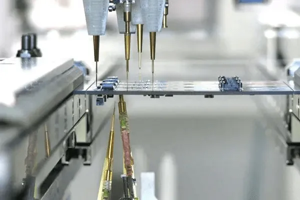
Electrical testing verifies circuit continuity and insulation resistance using methods like flying probe or bed of nails testing. Impedance testing is also crucial for high speed HDI designs to ensure signal integrity. Guidelines from IPC 9252 help define test parameters, ensuring boards perform reliably under specified electrical conditions.
Thermal and Environmental Testing
HDI PCBs often operate in harsh environments, requiring testing for thermal cycling and humidity resistance. Standards like IPC TM 650 provide methodologies for evaluating board performance under stress. These tests simulate real world conditions to predict long term reliability and prevent failures in the field.

Building a Reliable HDI PCB Testing and Inspection Workflow
Implementing effective quality control for HDI PCBs requires a proactive approach, integrating best practices across design, manufacturing, and testing phases. Electrical engineers can adopt the following strategies to enhance reliability and performance.
Design for Manufacturability (DFM)
Incorporate DFM principles during the design stage to minimize manufacturing challenges. This includes optimizing microvia placement, ensuring adequate trace spacing, and selecting compatible materials. Adhering to IPC 2226 guidelines for HDI design helps avoid common pitfalls that lead to quality issues.
Process Monitoring and Control
Continuous monitoring of manufacturing processes, such as etching, drilling, and lamination, prevents deviations that affect quality. Statistical process control techniques can identify trends or anomalies, allowing for timely corrective actions. Compliance with ISO 9001:2015 for quality management systems supports consistent process execution.
Collaboration Across Teams
Effective communication between design, manufacturing, and testing teams ensures that quality requirements are understood and met at every stage. Sharing inspection data and test results fosters a collaborative environment, reducing the risk of overlooked defects in HDI PCB production.
Solving Testing Challenges in High-Reliability HDI PCB Manufacturing
HDI PCBs present unique challenges due to their complexity, such as detecting internal defects or managing tight tolerances. One common issue is microvia reliability, where poor drilling or plating can lead to connection failures. Using advanced X ray inspection and adhering to IPC 6012E criteria can mitigate this risk by ensuring via integrity.
Another challenge is maintaining signal integrity in high speed designs. Inconsistent impedance or crosstalk can degrade performance. Electrical testing based on IPC 9252 standards, combined with precise design practices, helps address these issues. Engineers should also prioritize material selection to match dielectric properties with design requirements.
High-reliability HDI PCB applications require testing strategies that go beyond basic continuity checks. Microvia structures, sequential buildup layers, fine-line routing, and dense interconnects can introduce failure mechanisms that are not always visible during conventional inspection. Depending on the application, reliability evaluation may therefore combine electrical testing, thermal cycling, X-ray inspection, microsection analysis, and other qualification methods.
Conclusion
Quality control for HDI PCBs is a multifaceted process that demands attention to detail, adherence to industry standards, and the use of advanced testing methods. By implementing robust HDI PCB quality control methods and inspection criteria, electrical engineers can ensure reliability and performance in complex electronic systems. From material verification to electrical testing, each step plays a critical role in delivering boards that meet stringent demands. Staying aligned with standards like IPC 6012E and IPC A 600K provides a solid foundation for consistent quality, enabling innovation in high density interconnect designs.
FAQ
Q1: What Is HDI Testing?
A1: HDI testing is the process of verifying the electrical and reliability performance of high-density interconnect PCBs. It can include continuity testing, insulation resistance testing, impedance verification, thermal cycling, and other evaluations depending on the board design. HDI testing works together with visual and dimensional inspection to identify defects that may affect microvias, fine traces, interconnections, and overall PCB performance.
Q2: What Is the Difference Between HDI Testing and HDI Inspection?
A2: HDI inspection primarily evaluates the physical condition and structural accuracy of a PCB, while HDI testing verifies electrical or environmental performance. HDI inspection may use AOI, microscopy, X-ray, and dimensional measurement, whereas testing can include continuity, insulation resistance, impedance, and thermal evaluations. Using both approaches provides broader quality control for complex HDI PCB structures.
Q3: What Inspection Methods Are Used for HDI PCBs?
A3: Common HDI inspection methods include visual inspection, automated optical inspection, X-ray inspection, dimensional measurement, microscopic analysis, and cross-section evaluation. AOI is useful for detecting visible surface defects, while X-ray inspection can examine internal structures such as microvias and buried interconnections. The appropriate HDI inspection method depends on board construction, feature density, production volume, and applicable acceptance requirements.
Q4: How Do Automated Solutions Improve HDI PCB Inspection?
A4: Automated solutions for HDI PCB inspection improve consistency by using repeatable imaging and defect-detection processes. AOI systems can identify fine-line defects, missing features, solder mask irregularities, and other surface issues at production speed. Automated inspection can also generate process data that helps engineers identify recurring manufacturing trends and improve drilling, etching, lamination, and plating control.
Q5: What Testing Is Required for High-Reliability HDI PCBs?
A5: High-reliability HDI boards may require more extensive testing than basic production continuity checks. Depending on the application, engineers can combine electrical testing, X-ray inspection, microsection analysis, thermal cycling, humidity testing, and other qualification methods. These evaluations help assess potential failure mechanisms associated with microvias, multilayer interconnections, dielectric materials, and repeated thermal or environmental stress.
Q6: How Does HDI PCB Assembly Testing Differ From Bare-Board Testing?
A6: HDI PCB assembly testing evaluates the board after components have been mounted, while bare-board testing focuses on the fabricated PCB itself. Assembly testing can include solder-joint inspection, BGA X-ray inspection, electrical continuity, functional testing, and thermal evaluation. For dense HDI assemblies, combining board-level inspection with assembly testing helps identify defects introduced during component placement, soldering, or reflow.
Q7: What Standards Support HDI PCB Testing and Inspection?
A7: The source article identifies IPC standards including IPC-6012E, IPC-A-600K, IPC-9252, IPC-2226, IPC-4101E, and IPC-TM-650 as references for different aspects of PCB quality, design, materials, testing, and acceptability. The applicable requirements should be selected according to the board construction, customer specifications, and relevant industry requirements rather than treating one standard as sufficient for every HDI application.
References
IPC-6012E — Qualification and Performance Specification for Rigid Printed Boards. IPC, 2020.
IPC-A-600K — Acceptability of Printed Boards. IPC, 2020.
IPC-9252 — Requirements for Electrical Testing of Unpopulated Printed Boards. IPC, 2016.
IPC-2226 — Sectional Design Standard for High Density Interconnect (HDI) Printed Boards. IPC, 2003.
IPC-4101E — Specification for Base Materials for Rigid and Multilayer Printed Boards. IPC, 2017.
IPC-TM-650 — Test Methods Manual. IPC, 2021.
ISO 9001:2015 — Quality Management Systems. ISO, 2015.