 04:29
04:29
AOI Inspection
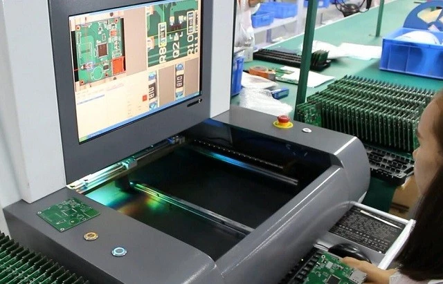
Automated Optical Inspection (AOI) plays a critical role in modern PCB manufacturing, serving as an essential quality control technique that uses high-resolution cameras and advanced algorithms to detect defects on assembled circuit boards. By automating the visual inspection process, AOI systems identify issues such as soldering errors, component misalignment, missing parts, and bridging, which are common challenges in high-volume production environments. For engineers, technicians, and manufacturers searching for AOI Inspection resources, this tag aggregates in-depth content that explains the fundamentals, from basic setup to sophisticated integration with other automated processes like SPI (Solder Paste Inspection) and ICT (In-Circuit Testing). Understanding AOI not only helps minimize rework and scrap rates but also ensures compliance with industry standards like IPC-A-610, ultimately boosting yield and reliability in electronic assemblies. Professionals often turn to AOI Inspection to optimize their workflows, and the articles here provide practical guidance on selecting the right AOI equipment based on factors such as board complexity, throughput requirements, and defect detection accuracy. For instance, implementing 3D AOI can offer superior analysis of solder joint volumes compared to traditional 2D methods, enabling early detection of subtle flaws that might lead to field failures. Best practices include calibrating systems regularly, training operators on false call reduction, and leveraging data analytics from AOI outputs to refine upstream processes like stencil printing or pick-and-place operations. Whether you're troubleshooting persistent defects in a prototype run or scaling up for mass production, the insights in these tagged articles can help you apply AOI effectively, reducing costs and enhancing product quality. Diving deeper into specific applications, such as AOI in automotive electronics or consumer devices, reveals how this technology adapts to diverse needs, including handling fine-pitch components and high-density interconnects. Readers interested in real-world case studies or comparisons with manual inspection methods will find valuable discussions that illustrate measurable improvements in efficiency and error rates. As PCB designs grow more intricate, staying informed on AOI advancements ensures your manufacturing line remains competitive and defect-free.
Video Guide
-
04:29
Technical Articles
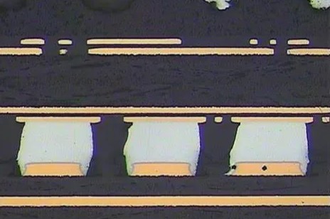
14 Common PCBA Test Methods
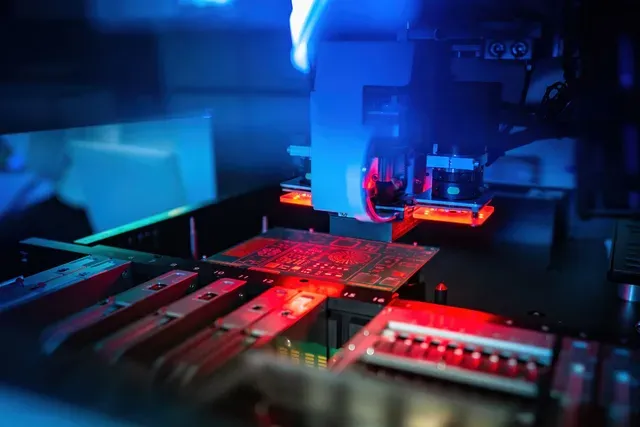
How Does Lighting Impact Automated Optical Inspection (AOI) for PCBs?
Avoid Costly Rework: Design for Testing (DFT) Strategies for IPC Compliant PCBs
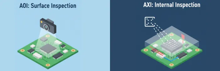
Visual Inspection Vs. Automated X Ray: Choosing the Right PCB Inspection Method
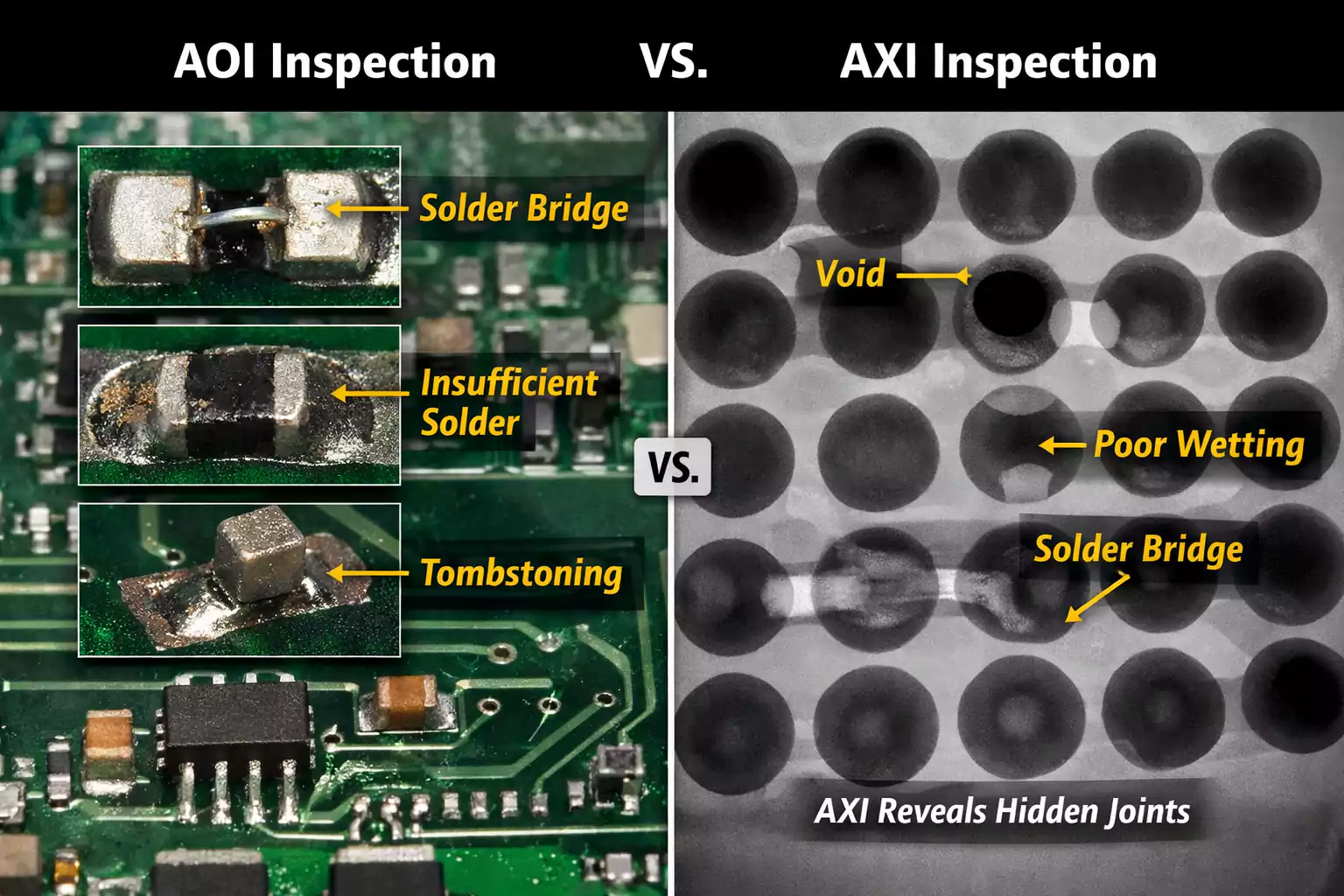
AOI vs. X Ray: Choosing the Right Solder Joint Inspection Method for Your PCB
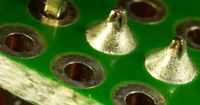
The Ultimate Guide to Solder Joint Inspection: Techniques, Tools, and Best Practices
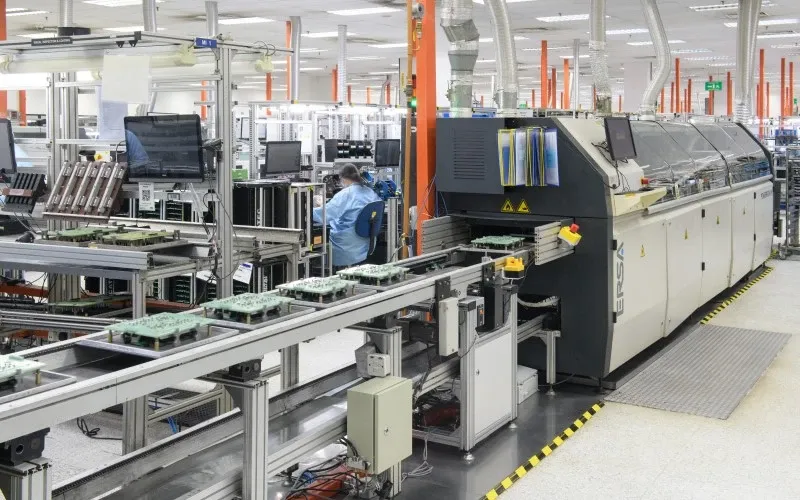
The Role of Automation in High Volume PCB Manufacturing: Improving Efficiency and Quality
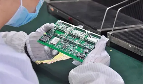
Top 7 PCB Testing Methods to Guarantee Quality and Reliability
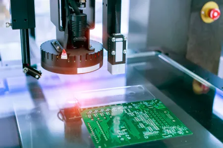
AOI Programming for Dummies: A Step by Step Guide to PCB Inspection
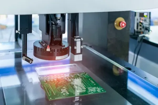
Selecting the Right PCB Inspection Equipment: A Guide to AOI, X Ray, and Flying Probe Testing
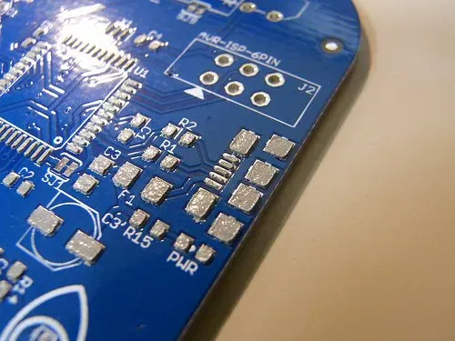
Blue Solder Mask for PCBs: Enhancing Contrast and Readability
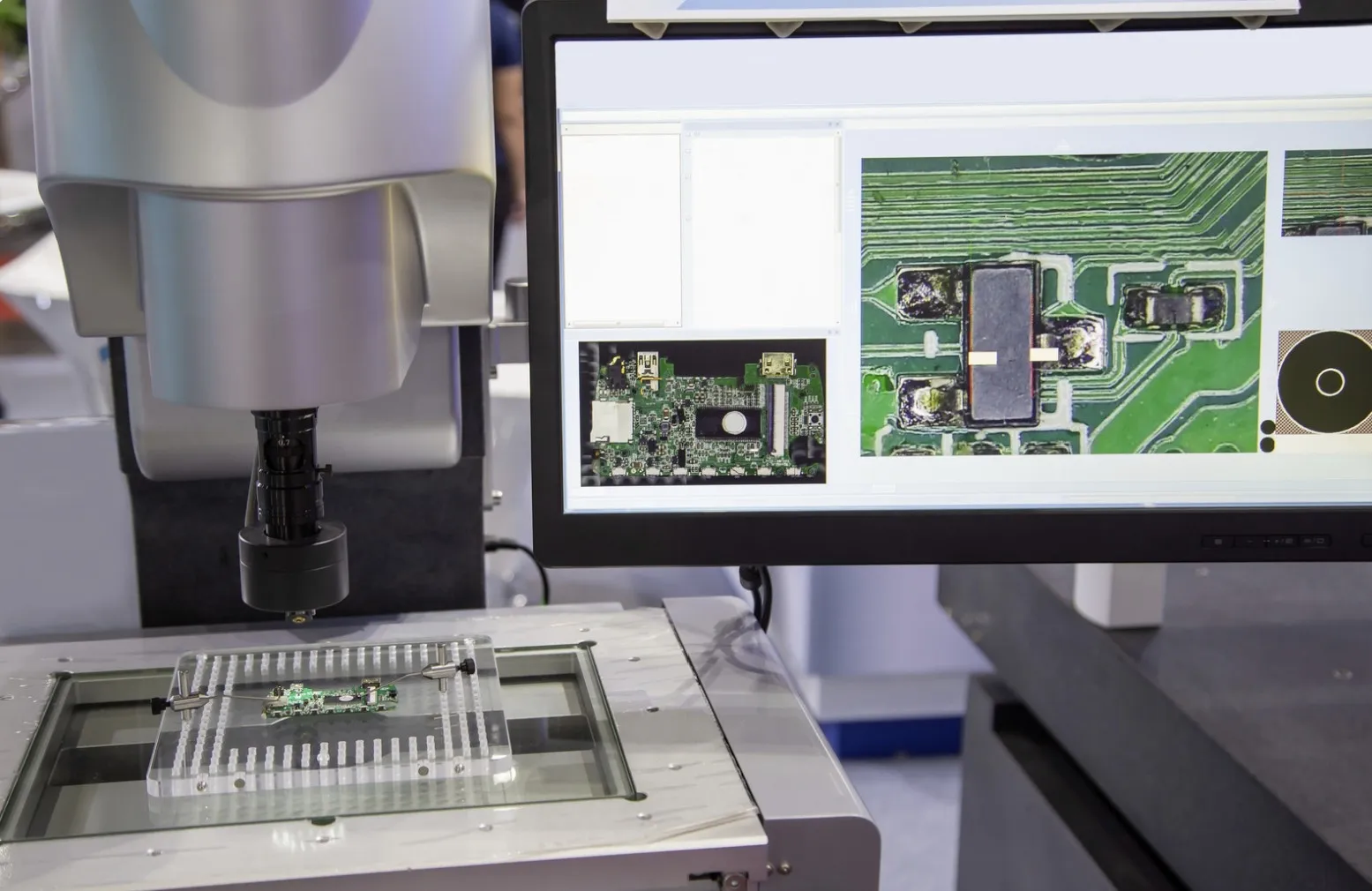
The PCB Imaging: Challenges Manufacturers Face With PCB Inspection
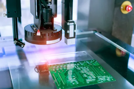
How AOI Equipment Detects Common PCB Defects: A Visual Guide
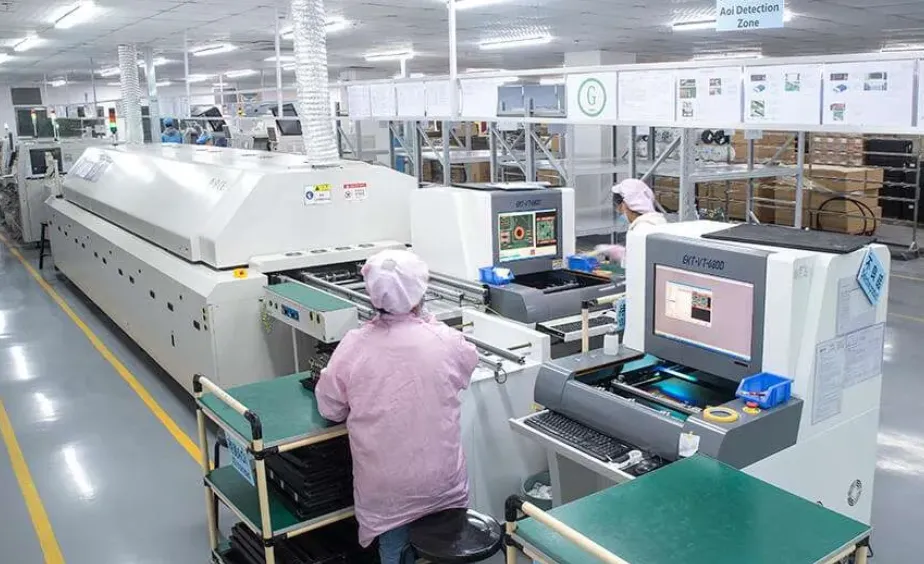
AOI Equipment Programming: A Step by Step Guide for Engineers
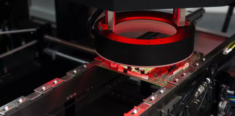
How AOI Equipment Can Reduce Defects and Improve Quality in PCB Manufacturing
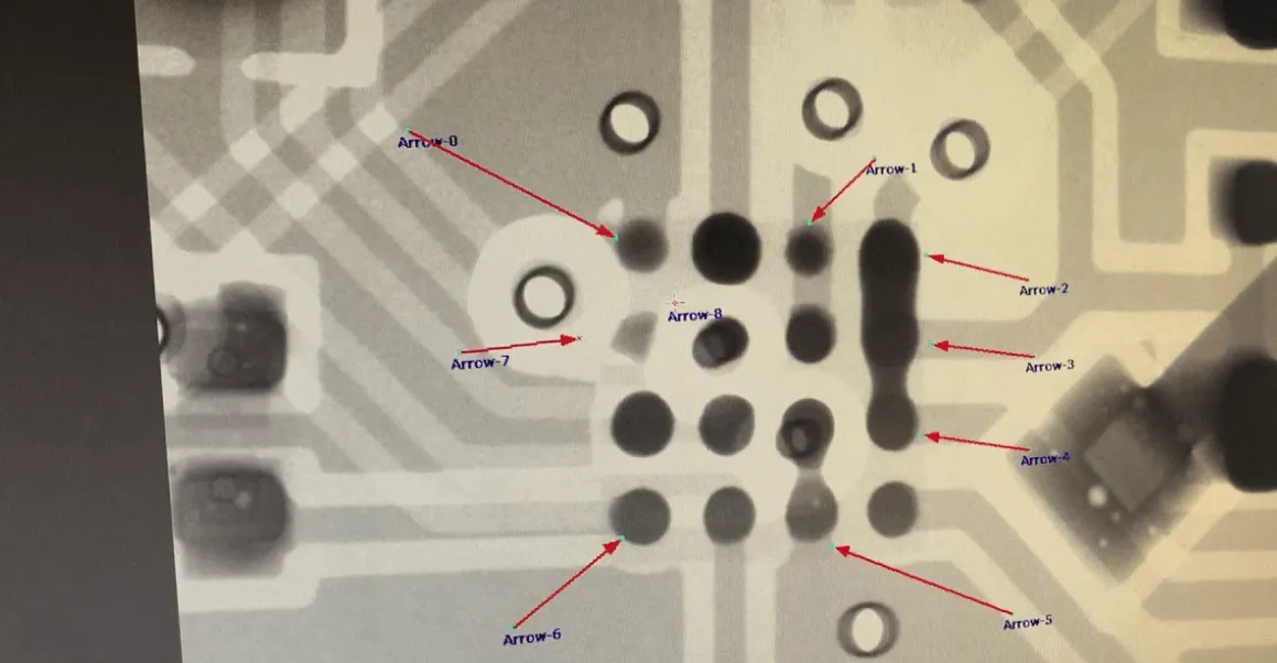
From AOI to AXI: Why X Ray Inspection is Crucial for Modern Electronics Manufacturing
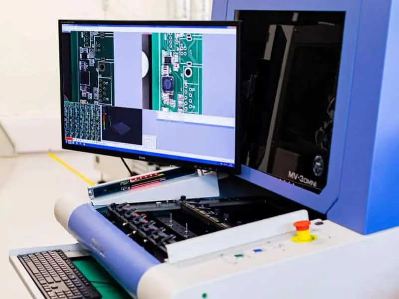
PCB Prototyping Assembly: Ensuring Quality with Automated Optical Inspection (AOI)
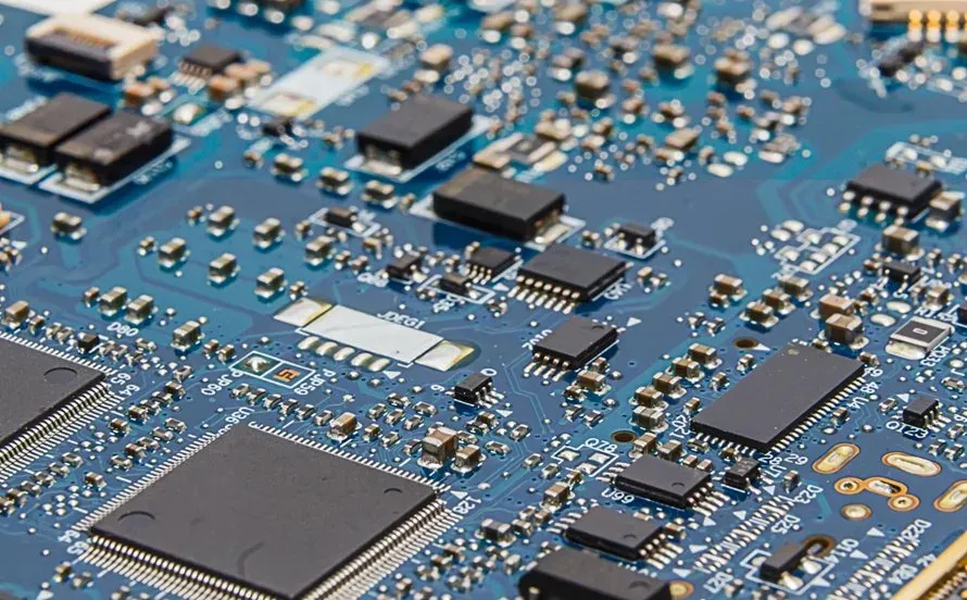
Troubleshooting SMT Assembly Defects: A Comprehensive Guide for Engineers
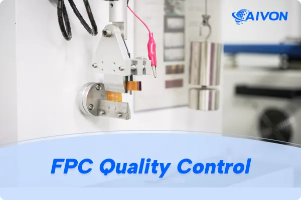
Quality Control in FPC Manufacturing: Key Inspection Points