Introduction
Printed circuit board (PCB) testing forms the cornerstone of quality control in electronics manufacturing, ensuring that boards meet performance expectations under real-world conditions. For electric engineers designing complex systems, selecting the right PCB testing methods prevents field failures, reduces rework costs, and upholds reliability standards. As production volumes increase and designs incorporate denser components, comprehensive testing becomes essential to detect defects early. This article explores the top seven PCB testing methods, from visual checks to advanced stress simulations, providing factory-driven insights aligned with industry practices. Each method addresses specific failure modes, such as soldering issues, electrical shorts, or component weaknesses. By integrating these into your quality assurance workflow, engineers can achieve higher yields and dependable assemblies.
Why PCB Testing Matters in Modern Electronics
PCB testing verifies that manufactured boards conform to design specifications and endure operational stresses. Defects like open circuits, misaligned components, or voids in solder joints can compromise system integrity, leading to costly recalls or safety risks. In high-reliability applications, such as automotive or aerospace electronics, rigorous PCB testing aligns production with standards like IPC-A-600K for acceptability criteria. Engineers benefit from layered testing strategies that combine optical, electrical, and environmental methods for full coverage. Ultimately, effective PCB testing minimizes variability, supports scalability, and ensures compliance with customer requirements.
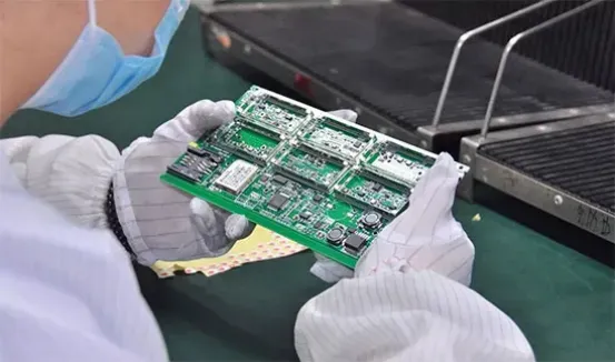
Visual Inspection: The First Line of Defense
Visual inspection remains a fundamental PCB testing method, relying on trained operators or basic magnification tools to identify surface-level defects. Engineers examine solder joints, component placement, and board cleanliness for issues like bridging, cracks, or contamination. This manual approach excels in low-volume prototypes where quick feedback is needed. It sets the baseline for automated methods by flagging obvious anomalies before further processing. While subjective, combining it with IPC-A-600K guidelines standardizes defect classification across teams. In factory settings, visual inspection catches up to 50 percent of assembly errors efficiently.
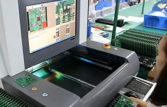
Automated Optical Inspection (AOI): Precision at Scale
Automated optical inspection (AOI) uses high-resolution cameras and algorithms to scan PCBs for defects in real time. Multiple angles and light sources reveal issues such as insufficient solder, tombstoning, or polarity errors that human eyes might miss. Ideal for high-volume surface-mount technology (SMT) lines, AOI processes boards at speeds exceeding thousands per hour. It compares captured images against golden samples or CAD data for pass-fail decisions. This PCB testing method integrates seamlessly post-reflow soldering, enhancing traceability through defect mapping. AOI significantly boosts first-pass yields by automating consistency checks.
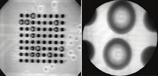
X-ray Inspection: Revealing Hidden Flaws
X-ray inspection penetrates opaque materials to visualize internal structures, making it indispensable for ball grid array (BGA) and multilayer boards. Engineers detect voids, head-in-pillow defects, or insufficient solder volume in hidden joints without disassembly. 2D or 3D imaging modes provide detailed cross-sections for precise analysis. This non-destructive PCB testing method suits double-sided assemblies where traditional optics fall short. Factories deploy it after reflow to validate underfill or via integrity. X-ray ensures reliability in dense packages by quantifying joint quality metrics.
In-Circuit Testing (ICT): Electrical Verification Fixture-Based
In-circuit testing (ICT) employs a bed-of-nails fixture to probe thousands of points, measuring resistance, capacitance, and voltage for component functionality. It powers up the board selectively to check passive and active parts against predefined limits. Best for medium-to-high volumes with stable designs, ICT achieves near-100 percent fault coverage on accessible nets. Engineers program test sequences based on netlists, isolating opens, shorts, or wrong values. Guided by IPC-9252 electrical test levels, this method minimizes false calls through guarded measurements. ICT streamlines production by providing actionable diagnostics for repair stations.
Flying Probe Testing: Flexible Alternative for Prototypes
Flying probe testing uses movable probes to contact test points dynamically, eliminating custom fixtures for low-volume or rapid-change scenarios. Up to eight probes navigate via CAD data, performing continuity, isolation, and parametric tests at speeds suitable for NPI builds. This PCB testing method adapts to double-sided boards and fine-pitch components without mechanical wear. It supports signature analysis for bare boards per IPC-9252 guidelines. Engineers appreciate its reprogrammability, reducing setup times from weeks to hours. Flying probe complements ICT by handling complex geometries economically.
Functional Testing: System-Level Assurance
Functional testing simulates end-use conditions by applying input signals and verifying outputs across the entire assembly. It exercises interconnects, power rails, and firmware interactions to confirm holistic performance. Unlike nodal tests, functional testing reveals interaction faults like timing issues or marginal components. Engineers develop custom jigs with interfaces for sensors or displays, often at room temperature initially. This method verifies design intent post-assembly, catching assembly-induced anomalies. In factories, it serves as the final gate before shipping certified products.
Burn-in Testing: Stressing for Longevity
Burn-in testing accelerates early-life failures by operating boards at elevated temperatures and voltages in environmental chambers. Components self-heal or reveal infant mortality defects under prolonged stress, typically 24 to 168 hours. JEDEC standards guide conditions for moisture sensitivity and thermal cycling integration. Electric engineers use it for mission-critical applications like servers or medical devices. Data logging tracks parametric drifts, informing reliability predictions. Burn-in elevates confidence by weeding out weak links before deployment.
Best Practices for Implementing PCB Testing Strategies
Layer these methods sequentially: start with visual and AOI for pre-reflow, add X-ray for BGAs, follow with electrical tests like flying probe or ICT, and conclude with functional and burn-in for validation. Customize based on board complexity, volume, and risk profile to optimize cost versus coverage. Maintain golden boards and regular calibration to sustain accuracy. Train teams on standard interpretations, such as IPC classes, for consistent decisions. Track defect Pareto charts to refine upstream processes like stencil design or paste printing. This integrated approach aligns factory output with engineering specifications reliably.
Conclusion
Mastering these top seven PCB testing methods empowers electric engineers to deliver robust, high-quality boards that withstand demanding environments. From AOI's optical precision to burn-in's reliability proofing, each technique targets unique failure modes for comprehensive assurance. Prioritizing standard-aligned practices minimizes escapes and accelerates time-to-market. Factories achieve superior yields by tailoring combinations to product needs. Invest in these PCB testing essentials to safeguard your designs against real-world challenges.
FAQs
Q1: What is the difference between in-circuit testing and flying probe testing?
A1: In-circuit testing uses a fixed fixture for high-speed, high-volume probing of electrical parameters, ideal for stable production runs. Flying probe testing employs movable probes without fixtures, offering flexibility for prototypes and design changes. Both verify continuity and component values, but flying probe reduces upfront costs while ICT excels in throughput. Choose based on volume and fixture feasibility for optimal PCB testing coverage.
Q2: When should automated optical inspection (AOI) be integrated into PCB testing?
A2: Deploy AOI post-solder paste inspection, reflow, and wave soldering to detect placement errors, solder defects, and bridges early. It shines in SMT lines for its speed and repeatability, complementing visual checks. Integrate before electrical tests to avoid processing bad boards. AOI aligns with high-volume needs, providing defect maps for root-cause analysis in PCB testing workflows.
Q3: How does X-ray inspection enhance PCB quality control?
A3: X-ray inspection uncovers hidden defects like BGA voids or via cracks invisible to optics, ensuring internal integrity. Use it for high-density interconnects and lead-free solders prone to head-in-pillow issues. Non-destructive imaging supports 3D reconstruction for precise measurements. This PCB testing method prevents reliability failures in multilayer designs by validating joint formation.
Q4: Why is burn-in testing critical for PCB reliability?
A4: Burn-in testing precipitates early failures through elevated stress, eliminating weak components before field use. It simulates accelerated aging per JEDEC guidelines, monitoring voltage, temperature, and current drifts. Essential for automotive and telecom boards, it boosts mean time between failures. Combine with functional tests for comprehensive assurance in demanding applications.
References
IPC-A-600K — Acceptability of Printed Boards. IPC, 2020
IPC-9252B — Electrical Test Methods for Printed Boards. IPC, 2016
IPC-6012E — Qualification and Performance Specification for Rigid Printed Boards. IPC, 2017
JEDEC J-STD-020E — Moisture/Reflow Sensitivity Classification of Nonhermetic Surface Mount Devices. JEDEC, 2014


