Introduction
Solder joint inspection stands as a critical step in printed circuit board assembly, ensuring the integrity and longevity of electronic products. Poor solder joints can lead to intermittent failures, reduced reliability, and costly rework in high-volume production environments. This comprehensive guide explores solder joint inspection methods, tools, and best practices tailored for electrical engineers seeking precise quality control. From visual assessments to advanced imaging techniques, understanding these approaches helps maintain compliance with industry benchmarks. Factory teams rely on systematic inspection to detect defects early, minimizing downtime and enhancing product performance. By mastering the solder joint inspection process, engineers can optimize assembly lines for consistent results.
Why Solder Joint Inspection Matters
Solder joints form the electrical and mechanical connections between components and the PCB, making their quality paramount for device functionality. Defects such as voids, cracks, or insufficient wetting compromise signal integrity and thermal performance, potentially causing field failures. In high-reliability applications like aerospace or medical devices, rigorous inspection prevents catastrophic outcomes and supports warranty claims. Production data shows that early detection through solder joint inspection reduces scrap rates and rework costs significantly. Engineers must prioritize this process to align with end-user expectations for durability. Ultimately, effective inspection bridges manufacturing precision with real-world reliability.
Inspection also facilitates process optimization, allowing teams to refine reflow profiles or stencil designs based on defect patterns. Compliance with established criteria ensures assemblies meet performance thresholds across product lifecycles. For electrical engineers, integrating inspection data into design feedback loops accelerates improvements. This proactive stance differentiates high-quality factories from average ones.
Understanding Quality Criteria for PCB Solder Appearance Inspection
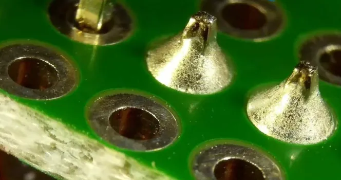
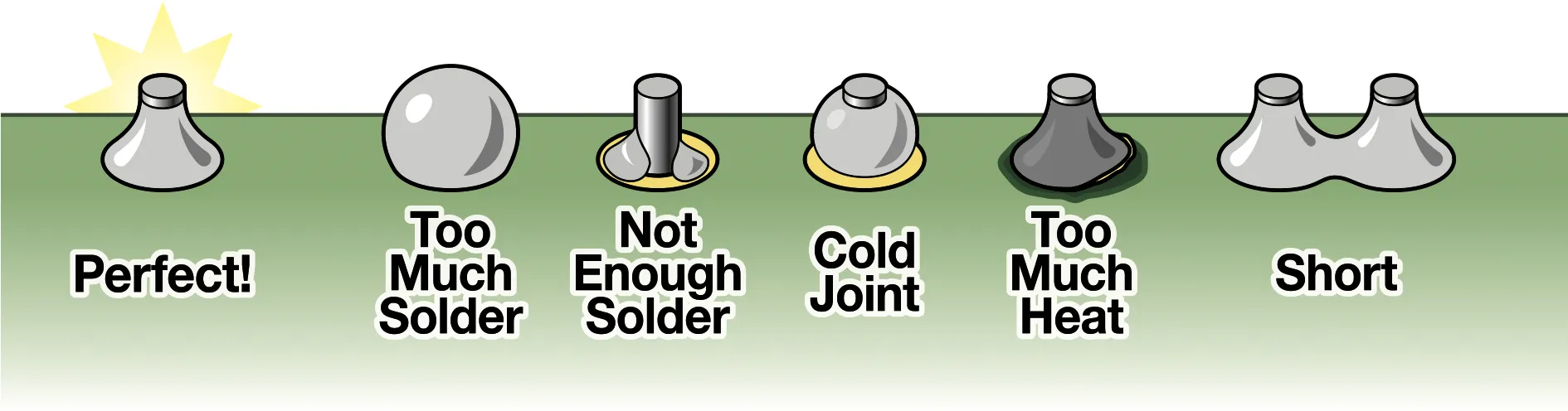
A quality solder joint exhibits proper wetting, where solder flows evenly over leads and pads, forming a smooth concave fillet. According to IPC-A-610, acceptable joints show no more than 25 percent voiding in certain configurations and maintain heel and toe fillet coverage. Electrical engineers evaluate factors like intermetallic compound formation, which ensures long-term adhesion without excessive growth that could embrittle the joint. Solder volume must align with pad size, avoiding bridges or insufficiencies that alter electrical paths. Surface finish compatibility, such as HASL or ENIG, influences inspection outcomes by affecting spreadability.
Classifications under IPC-A-610 define tolerances: Class 2 for general electronics allows minor imperfections, while Class 3 demands near-perfect joints for mission-critical use. Engineers assess wetting angle, ideally under 90 degrees, to confirm flux efficacy and reflow adequacy. Joint appearance provides clues to underlying issues like contamination or thermal mismatch. Consistent criteria application across inspections standardizes quality judgments in factory settings.
Solder Joint Inspection Methods
Solder joint inspection methods range from basic visual checks to sophisticated non-destructive techniques, each suited to specific defect types and production scales. Manual visual inspection serves as the first line of defense, relying on trained operators to spot obvious issues like bridging or tombstoning under adequate lighting. For higher precision, magnified visual methods use optics to reveal subtle cracks or dewetting. Automated optical inspection (AOI) employs cameras and algorithms to scan thousands of joints per minute, ideal for high-volume SMT lines.
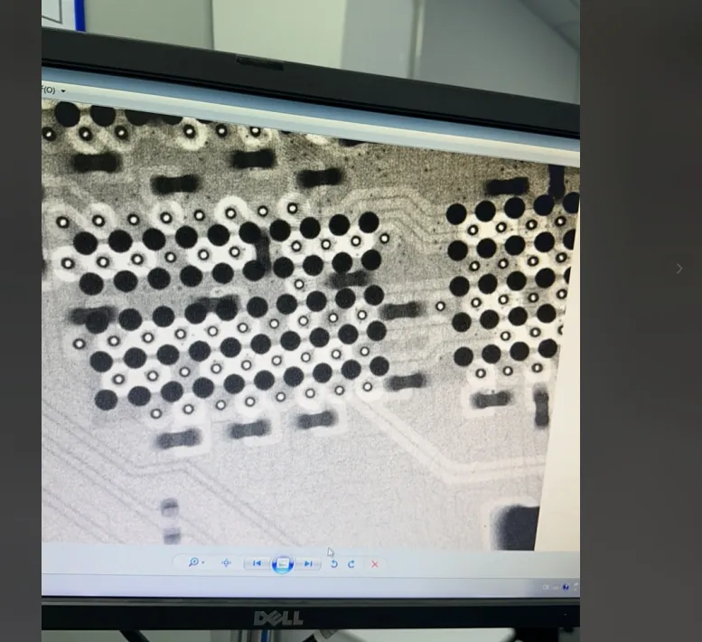
X-ray inspection, or automated X-ray (AXI), penetrates opaque packages like BGAs to detect voids, head-in-pillow defects, or missing balls hidden from surface views. Endoscopic borescopes access tight spaces for real-time internal joint evaluation. Ultrasonic and acoustic microscopy send sound waves to map voids or delaminations non-destructively. Destructive cross-sectioning, involving polishing and metallographic analysis, provides ultimate verification but suits sampling only.
Each method complements others: AOI handles topside defects efficiently, while AXI targets undersides. Engineers select based on component density and risk profile. Combining techniques maximizes coverage without excessive cycle time.
Suggested Reading: AOI vs. X Ray: Choosing the Right Solder Joint Inspection Method for Your PCB
Essential Tools for Your Solder Joint Inspection System
Solder joint inspection tools evolve with technology, offering scalability from benchtop to inline systems. Stereo microscopes with 10x to 50x magnification enable detailed manual checks, often paired with ring lights for shadow-free illumination. Digital microscopes add image capture and measurement software for documentation and analysis. AOI machines integrate multiple cameras, LED lighting, and AI-driven defect classification for 100 percent inspection.
X-ray systems, including 2D and 3D computed tomography units, reveal subsurface anomalies with high resolution. Flexible endoscopes with LED tips navigate under components for hidden joint views. Ultrasonic scanners provide thickness mapping for lead-free joints prone to cracking. Software platforms aggregate data from these tools, generating yield reports and trend analysis.
Selection criteria include throughput, resolution, and integration with existing lines. Electrical engineers prioritize tools supporting IPC-A-610 class-specific criteria.
Step-by-Step Solder Joint Inspection Process
The solder joint inspection process begins with preparation: clean the assembly if needed and ensure stable fixturing to avoid movement artifacts. Start with unaided visual scan for gross defects like excess solder or misalignment, progressing to 10x magnification for fillet integrity. Document findings with photos, noting locations per IPC-A-610 guidelines. For high-density boards, deploy AOI post-reflow to flag anomalies algorithmically.
Next, sample critical components like BGAs with AXI, verifying ball shear and void percentages. Use endoscopy for connectors or cavities inaccessible to overhead tools. Perform functional testing alongside to correlate visual data with electrical performance. Compile reports, categorizing defects by type and severity for root cause analysis.
This solder joint inspection tutorial emphasizes sequencing: pre-reflow SPI verifies paste, inline AOI catches post-placement shifts, and final AXI confirms hidden quality. Engineers iterate based on false calls, refining algorithms or lighting.
Solder Joint Inspection Best Practices
Adopt IPC J-STD-001 process controls to preempt defects, ensuring consistent preheat and peak temperatures during reflow. Standardize lighting at 1000 lux minimum with diffuse sources to eliminate glare on shiny surfaces. Train inspectors to IPC-A-610 criteria, using reference samples for calibration. Implement multi-stage inspection: 100 percent AOI plus targeted AXI for high-risk areas.
Log all data digitally for traceability, applying statistical process control to track CpK values. Minimize handling to prevent electrostatic damage during checks. Regularly validate tools against known standards.
Common Solder Joint Defects and Troubleshooting
Common solder joint defects include insufficient solder, causing open circuits, or bridging that shorts adjacent pads. Voids from flux entrapment weaken thermal paths, detectable via X-ray. Cracks from thermal cycling demand process tweaks like slower cooling. Head-in-pillow occurs in lead-free alloys, addressed by profile optimization.
Troubleshoot by correlating defects to process steps: poor wetting signals pad contamination, while tombstoning indicates paste volume imbalance. Cross-section high-failure samples for confirmation.
Conclusion
Mastering solder joint inspection methods, tools, and best practices elevates PCB assembly quality and reliability. Electrical engineers benefit from structured processes aligned with IPC standards, reducing failures downstream. Integrate these techniques for efficient, factory-ready workflows.
FAQs
Q1: What are the primary solder joint inspection methods for SMT assemblies?
A1: Solder joint inspection methods include visual, AOI, and X-ray techniques. Visual checks identify surface defects quickly, AOI automates high-volume scanning, and X-ray reveals BGA voids. Combine them for comprehensive coverage per IPC-A-610. This multi-method approach ensures process reliability in production.
Q2: Which solder joint inspection tools are best for high-density PCBs?
A2: For high-density PCBs, AOI systems and AXI tools excel in solder joint inspection. Microscopes suit manual verification, while endoscopes access hidden areas. Select based on throughput needs and defect types targeted.
Q3: What does the solder joint inspection process involve step-by-step?
A3: The process starts with visual preparation, followed by magnified checks, AOI scanning, and AXI for subsurface issues. Document and analyze data against standards. This tutorial ensures thorough quality assurance.
Q4: How can engineers implement solder joint inspection best practices?
A4: Best practices include standardized lighting, multi-tool integration, and IPC training. Monitor trends with SPC for continuous improvement. These steps optimize factory yields effectively.
References
IPC-A-610G - Acceptability of Electronic Assemblies. IPC, 2017
IPC J-STD-001G - Requirements for Soldered Electrical and Electronic Assemblies. IPC, 2017


