Introduction
Lead-free assembly has transformed industrial electronics manufacturing, driven by global regulations restricting hazardous substances. In harsh environments such as oil and gas facilities, heavy machinery, and transportation systems, lead-free industrial PCBs must withstand extreme temperatures, mechanical shock, vibration, and corrosive humidity. The shift from traditional tin-lead solders to lead-free alternatives introduces higher processing temperatures, which can exacerbate issues like board warpage and component stress if not managed properly. Engineers face the task of balancing compliance with enhanced reliability for long-term performance. This article delves into practical strategies for lead-free industrial soldering, component selection, and process optimization tailored to demanding industrial applications.
Why Lead-Free Assembly Matters in Industrial Applications
Industrial electronics operate in conditions far beyond consumer-grade specifications, where failures can lead to costly downtime or safety risks. Lead-free industrial components and soldering ensure environmental compliance while maintaining structural integrity under thermal cycling and mechanical loads. Unlike tin-lead solders, lead-free alloys offer superior resistance to thermal fatigue in many scenarios, making them suitable for high-reliability needs. Compliance with standards like IPC J-STD-001 for soldered assemblies guarantees consistent quality across production runs. Moreover, lead-free processes reduce long-term environmental impact without sacrificing the durability required in industrial settings. Engineers must prioritize these assemblies to meet both regulatory and operational demands effectively.
Technical Challenges of Lead-Free Soldering in Harsh Environments
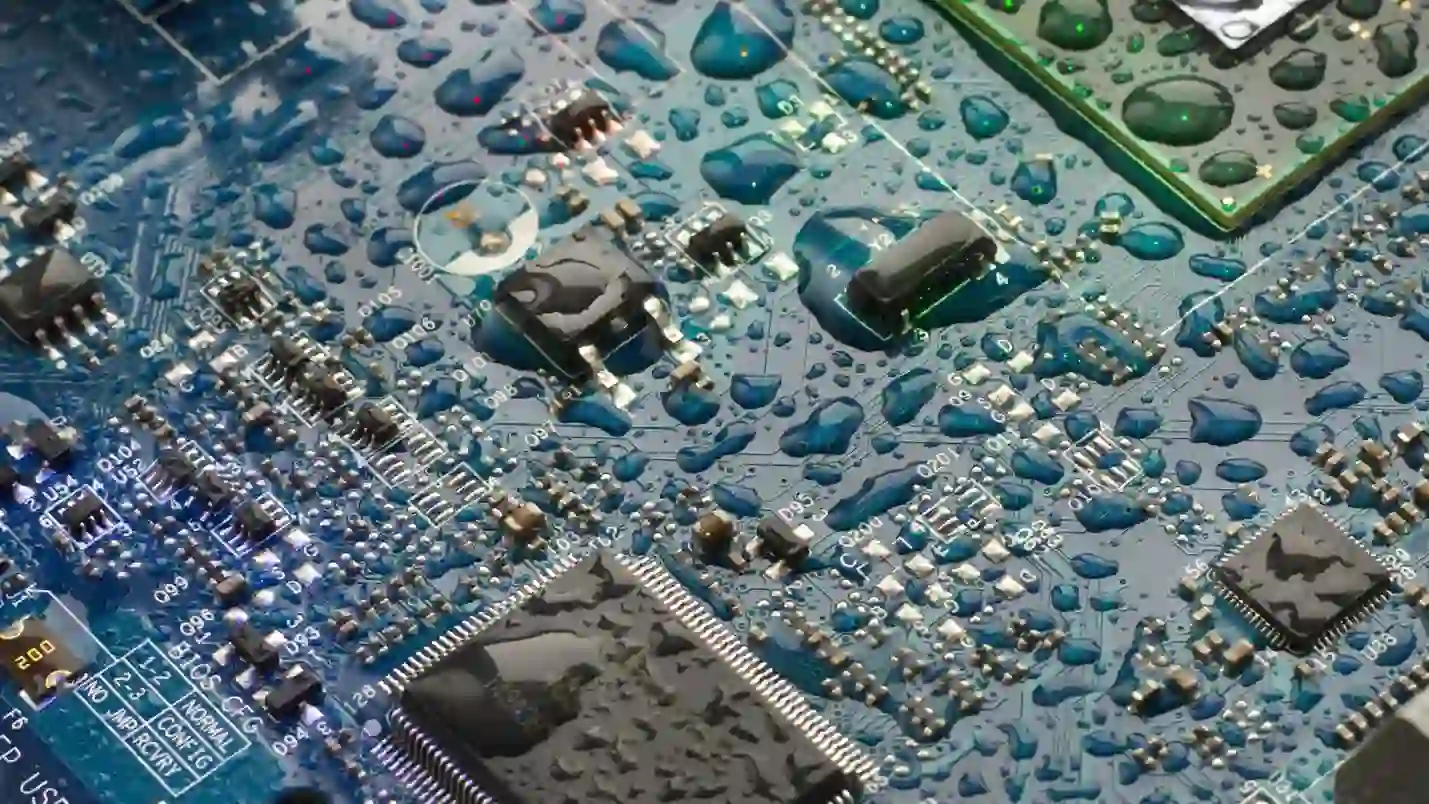
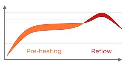
Lead-free solders, typically tin-silver-copper alloys, have higher melting points around 217 to 220 degrees Celsius compared to 183 degrees Celsius for tin-lead eutectics, necessitating reflow peaks up to 250 degrees Celsius. This elevation stresses PCBs, leading to warpage, delamination, or pad lifting, especially in thicker boards used for industrial power electronics. Vibration and shock in harsh environments accelerate fatigue cracking at solder joints, where the brittle intermetallics in lead-free alloys can propagate failures faster than in ductile tin-lead joints. Humidity introduces corrosion risks, as flux residues from lead-free processes are harder to clean completely. JEDEC J-STD-020 guidelines for moisture sensitivity help mitigate reflow-related damage, but industrial designs require additional precautions. These challenges demand a holistic approach from material selection through testing.
Material Selection for Lead-Free Industrial PCBs and Components
Choosing robust substrates is critical for lead-free industrial PCBs, with high glass transition temperature (Tg) materials resisting deformation during elevated reflow. Components must be rated for lead-free industrial soldering, featuring finishes like immersion tin or ENIG that promote wetting without excessive intermetallic growth. Solder pastes formulated for no-clean processes minimize residues that could corrode under humid conditions. Reinforcement with via-in-pad designs or metal-backed cores enhances vibration resistance in power-heavy industrial electronics. Always verify supplier datasheets align with IPC standards for high-reliability Class 3 assemblies. Proper selection prevents common pitfalls like tombstoning or insufficient hole fill in through-hole lead-free industrial soldering.
Optimizing the Lead-Free Assembly Process
Reflow profiling is the cornerstone of successful lead-free industrial soldering, requiring a gradual ramp-up to avoid thermal shock. Peak temperatures should stay within component tolerances, with controlled cooling to form reliable intermetallics without brittleness. For wave soldering in mixed assemblies, low-silver alloys improve hole fill while maintaining joint strength. Nitrogen atmospheres reduce oxidation, ensuring uniform wetting on lead-free industrial components. Stencil design with finer apertures prevents bridging on dense boards. Process validation through profilometers confirms adherence to JEDEC J-STD-020 moisture/reflow classifications, safeguarding against popcorn effects in humid storage.
Best Practices for Reliability in Harsh Environments
Post-assembly, conformal coatings shield lead-free industrial PCBs from moisture and contaminants, extending life in corrosive atmospheres. Mechanical fastening or potting secures boards against vibration, distributing stress away from solder joints. Accelerated life testing simulates harsh conditions, revealing weaknesses in lead-free joints early. Strain gauging during assembly monitors warpage, allowing iterative improvements. Integrating these practices ensures industrial electronics exceed operational lifecycles. Regular audits against IPC J-STD-001 criteria maintain process repeatability across volumes.
Troubleshooting Common Issues in Lead-Free Industrial Assembly
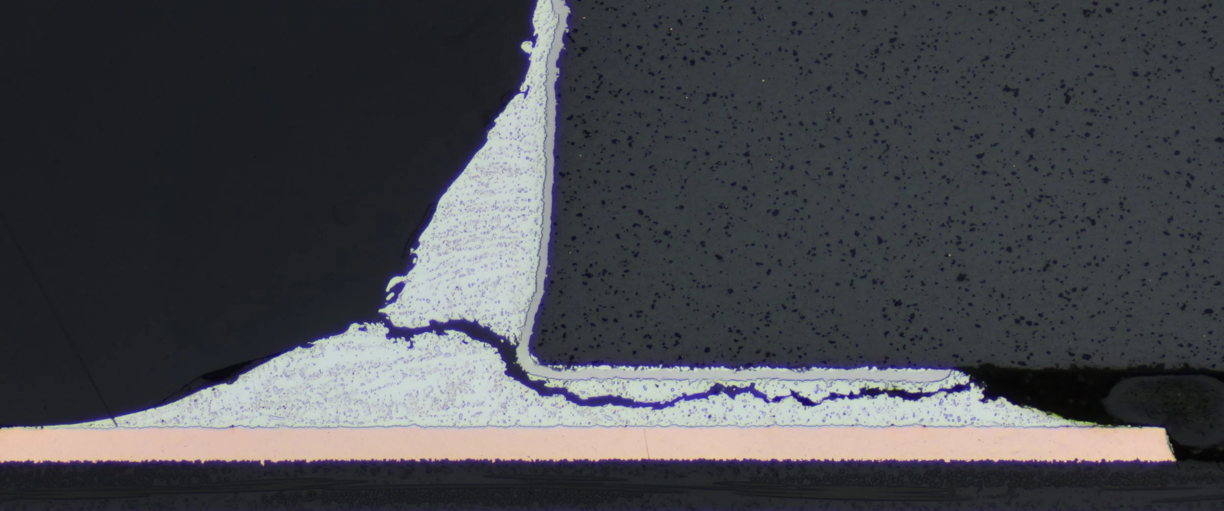
Tombstoning often stems from uneven heating; balance paste volume and reflow soak times to resolve it. Voids in BGA balls indicate trapped flux gases, mitigated by vacuum reflow or optimized paste printing. Head-in-pistol defects in wave soldering arise from poor flux activation, corrected with higher-activity formulations suited to lead-free alloys. Vibration-induced cracks show as daisy-chaining; reinforce with underfill or larger standoffs. Humidity failures present as dendritic growth; thorough cleaning and baking per JEDEC standards prevent them. Systematic root-cause analysis, including X-ray and cross-sectioning, guides fixes for sustained reliability.
Case Insights: Enhancing Durability Through Integrated Design
In applications like motor controls, combining high-Tg laminates with lead-free industrial components reduced failure rates under thermal-vibration cycles. Designers iterated reflow profiles to minimize CTE mismatch, preserving joint integrity. Conformal coatings proved essential against salt fog exposure. These approaches, grounded in standards, yielded assemblies outperforming expectations in field trials. Troubleshooting focused on real-time monitoring prevented escalation of minor defects.
Conclusion
Optimizing lead-free assembly for industrial applications hinges on meticulous material choices, precise process controls, and rigorous testing. Lead-free industrial PCBs and soldering deliver compliance and reliability when tailored to harsh realities like extreme temperatures and vibration. By following best practices and standards, engineers can achieve robust industrial electronics that endure demanding service. Proactive troubleshooting ensures minimal downtime and maximum longevity. Embracing these strategies positions teams for success in evolving regulatory landscapes.
FAQs
Q1: What are the main challenges with lead-free industrial soldering in high-vibration environments?
A1: Lead-free alloys' higher melting points increase reflow stresses, potentially weakening joints under vibration. Brittle intermetallics accelerate cracking compared to tin-lead. Select vibration-rated lead-free industrial components and use mechanical reinforcements like potting. Adhere to IPC J-STD-001 for joint criteria to enhance fatigue resistance.
Q2: How do you select lead-free industrial components for harsh temperature swings?
A2: Prioritize components with finishes enduring 260-degree Celsius peaks per JEDEC J-STD-020. Verify MSL ratings and high-Tg compatibility to avoid damage. Test for thermal cycling per industry specs. This ensures reliable lead-free industrial PCB performance in extremes.
Q3: What best practices optimize reflow for lead-free industrial PCBs?
A3: Develop profiles with slow ramps, precise peaks, and nitrogen use to prevent oxidation. Use high-Tg boards and validated stencils for uniform heating. Profile every run to match lead-free industrial soldering needs, reducing defects like warpage.
Q4: Why is conformal coating critical for lead-free industrial electronics?
A4: It protects solder joints from humidity-induced corrosion, common with lead-free flux residues. Coatings also buffer vibration and thermal shock. Apply post-cleaning per standards for optimal adhesion in harsh environments.
References
IPC J-STD-001G — Requirements for Soldered Electrical and Electronic Assemblies. IPC, 2017
JEDEC J-STD-020E — Moisture/Reflow Sensitivity Classification of Nonhermetic Surface Mount Devices. JEDEC, 2014
IPC-6012DS — Qualification and Performance Specification for Rigid Printed Boards in High Reliability Applications. IPC, 2015


