Introduction
Electronics hobbyists often spend hours assembling printed circuit boards by hand, only to face frustrating issues like intermittent connections or complete failures. These problems frequently stem from solder joint defects, which can undermine even the most carefully designed projects. A reliable solder joint defects visual guide helps you spot these issues early, saving time and materials during prototyping. By learning to identify bad solder joint examples through simple visual checks, you gain the confidence to troubleshoot and refine your soldering technique. This guide focuses on common solder joint problems tailored for hobbyist workflows, using magnification and good lighting as key tools. Mastering solder joint defects identification ensures your circuits perform reliably from the first power-up.
Visual inspection remains the quickest and most accessible method for hobbyists to assess joint quality without specialized equipment. Standards like IPC-A-610J provide benchmarks for what constitutes acceptable joints across different classes, from general hobby use to more demanding applications. Whether you are populating a simple Arduino shield or a custom sensor board, recognizing how to identify solder defects prevents costly rework. This article breaks down the most frequent issues with practical descriptions, causes, and fixes, empowering you to achieve professional results at home.
What Are Solder Joint Defects and Why Do They Matter?
Solder joint defects occur when the metallurgical bond between a component lead, pad, and solder fails to form properly, leading to weak electrical or mechanical connections. In hobbyist projects, these defects manifest as no connectivity, high resistance, or joints that crack under vibration. Common solder joint problems include poor wetting, excess material, or incomplete reflow, each with distinct visual cues that this solder joint defects visual guide highlights. Understanding them matters because unreliable joints cause 70 percent of field failures in electronics assemblies, turning a fun build into a debug nightmare.
For hobbyists, bad solder joints often result from hand soldering variables like iron temperature or flux application, unlike automated reflow in production. They compromise signal integrity, especially in high-frequency circuits, and accelerate under thermal cycling. IPC J-STD-001J outlines requirements for materials and processes to minimize these risks, offering criteria adaptable to benchtop setups. By prioritizing solder joint defects identification, you extend project lifespan and build skills transferable to collaborative or professional work. Early detection via visual checks keeps your focus on innovation rather than repair.
Common Solder Joint Defects: Visual Identification Guide
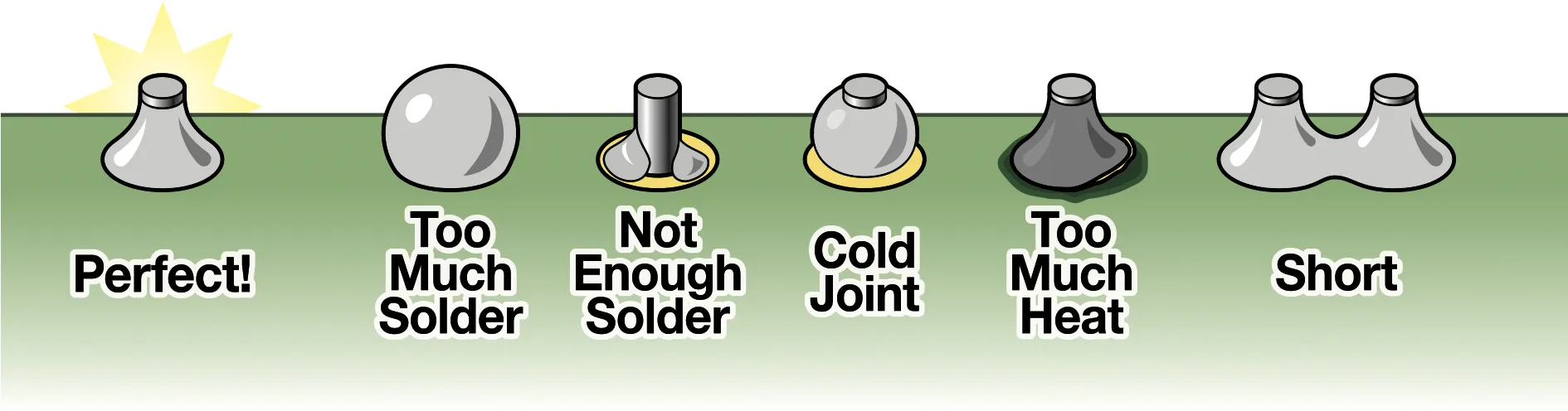
Spotting solder defects starts with knowing what a good joint looks like: smooth, shiny, concave fillet covering the lead and pad fully, with no gaps or cracks. Deviations signal issues, and this section details bad solder joint examples with troubleshooting cues. Use a 10x magnifier and oblique lighting to reveal surface textures and contours. Hobbyists benefit from comparing your work against these descriptions during and after soldering. Deviations signal issues, and this section details bad solder joint examples with troubleshooting cues. See related SMT assembly defects for production-scale context.
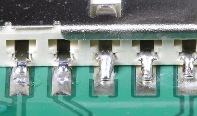
Cold Solder Joints
A cold solder joint appears dull and grainy, lacking the smooth, mirrored shine of a proper bond. The solder looks rough or pockmarked, as if frozen mid-flow, with poor wetting where it barely adheres to the lead or pad. This defect arises from insufficient heat, causing incomplete melting and reflow, resulting in high-resistance connections that fail intermittently. To identify it in your solder joint defects visual guide checks, tilt the board; the joint will not reflect light evenly and may show a ring around the lead base.
Fix by reheating with fresh flux to achieve proper melting, ensuring the iron tip wets the joint fully for 2–3 seconds. Prevention involves preheating components slightly and using irons at 350–400 degrees Celsius for lead-free solder. Cold joints plague beginners but become obvious with practice.
Solder Bridges
Solder bridges form when excess molten solder connects adjacent pads or pins unintentionally, creating shorts. Visually, they look like thin wires or blobs spanning gaps, often shiny but hazardous. In dense surface-mount boards, they mimic intended fillets but disrupt circuits, causing immediate power issues or erratic behavior. Check by powering off and inspecting under magnification; continuity tests confirm unwanted paths.
Causes include too much solder paste or dragging during hand soldering. Clean with desoldering braid and flux, then reapply precisely. IPC-A-610J classes these as defects unless isolated properly.
Insufficient Solder or Poor Wetting
Insufficient solder leaves joints skeletal, with exposed pad or lead bases not covered by at least 75 percent fillet. The solder bead sits high without flowing into contours, signaling dewetting where flux fails or surfaces oxidize. This weak spot breaks easily, ideal for vibration-sensitive hobby projects like drones. Look for dull edges or gaps in your how to identify solder defects routine.
Oxidized pads from storage cause this; clean with isopropyl alcohol and fresh flux. Apply minimal solder to encourage flow.
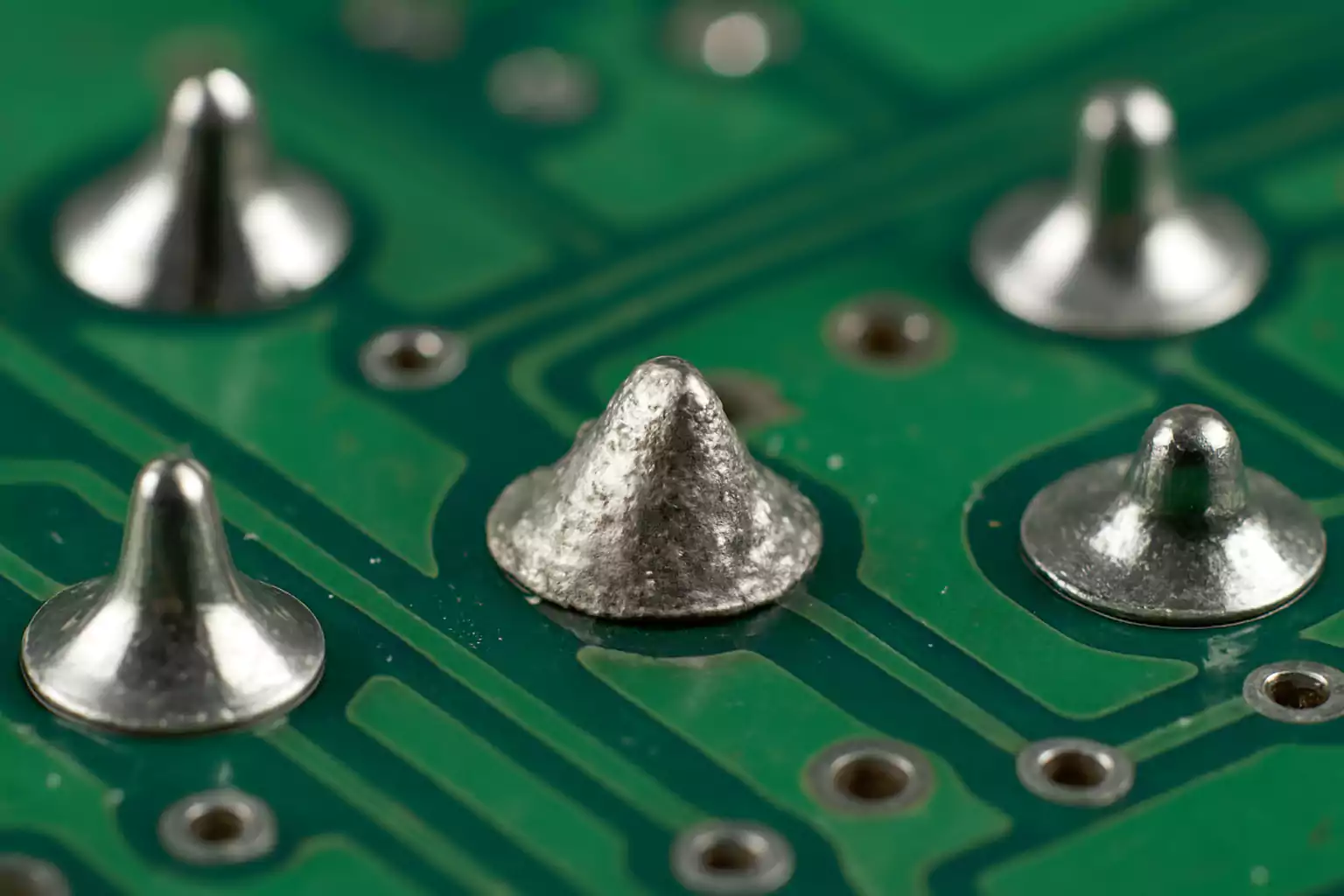
Excessive Solder
Excessive solder creates bulbous blobs engulfing leads, hiding pad contours and risking bridges. It appears piled up, often with icicles or spikes from rapid cooling. While mechanically strong, it traps flux residues leading to corrosion and complicates inspection. Measure visually: fillets should not protrude beyond pad edges significantly.
Trim with wick or hot air, but prevention via controlled paste volume works best for stencil users.
Tombstoning
Tombstoning happens in reflow or hand soldering where one component end lifts like a gravestone due to uneven heating. The lifted lead shows no solder contact, while the other wets fully, causing opens. Common in chip resistors, it stems from pad size mismatch or rapid preheat. Spot the vertical stance immediately post-solder.
Balance heating symmetrically and ensure equal pad solderability.
Solder Balls and Beads
Solder balls scatter as tiny spheres around joints from incomplete paste reflow or vibration during cooling. They migrate under voltage, shorting traces over time. Inspect clean areas post-assembly; beads adhere loosely.
Vacuum or brush away, preventing with stable profiles.
Cracked or Fractured Joints
Cracked joints show hairline fissures in fillets, often from mechanical stress or thermal shock. They start shiny but dull with lines, failing under flex. Vibration in enclosures exacerbates this.
Rework gently, avoiding torque.
Suggested Reading: Solder Joint Defects: Diagnosing & Fixing Common Soldering Issues
Causes of Solder Joint Defects
Most defects trace to process variables hobbyists control: iron temperature too low for cold joints, too high for bridges. Flux burnout from prolonged heat leads to poor wetting, while contaminated pads cause balls. Component misalignment during placement contributes to tombstoning. Humidity affects solderability, so store in dry boxes.
Surface finishes like HASL versus ENIG influence wetting; mismatched pairs amplify issues.
How to Identify Solder Defects: Practical Visual Inspection Tips
Start with bright, angled lighting to cast shadows revealing contours. A stereo microscope or loupe at 20–40x magnification exposes microcracks invisible to the eye. Inspect at multiple angles: top for bridges, side for fillet shape. Power-cycle tests complement visuals for intermittents.
Document with photos for before–after comparisons in your solder joint defects identification log.
Fixing and Preventing Bad Solder Joints
Reflow suspect joints with flux and iron, adding or removing solder as needed. For bridges, braid absorbs excess precisely. Prevention emphasizes clean tools, calibrated irons, and practice on scrap boards. Use quality lead-free solder with rosin core for hobby work.
Adopt IPC J-STD-001J principles: consistent heat, minimal disturbance.
Conclusion
This solder joint defects visual guide equips electronics hobbyists to spot and resolve common solder joint problems swiftly. From cold joints to bridges, visual cues guide your inspections, ensuring robust assemblies. Apply these insights to elevate your projects, reducing failures and boosting satisfaction. Regular practice turns defects into learning opportunities.
FAQs
Q1: What are the most common bad solder joint examples for beginners?
A1: Cold joints and solder bridges top the list in solder joint defects identification for hobbyists. Cold joints look dull and grainy from low heat, while bridges short circuits with shiny spans. Use magnification to confirm, then reheat with flux. Prevention involves steady iron temperature and precise application. This how to identify solder defects approach catches most issues visually.
Q2: How can I use a solder joint defects visual guide at home?
A2: Grab a magnifier, LED lamp, and oblique light for shadows on joints. Compare to good examples: shiny, smooth fillets. Check for dullness in cold joints or gaps in poor wetting per common solder joint problems. Tilt boards for 3D views. Practice on test strips builds intuition quickly.
Q3: What causes tombstoning in my hand-soldered boards?
A3: Uneven heating lifts one end during cooling, a frequent solder defect. Pads with unequal solder volume or rapid temperature ramps contribute. Ensure symmetric flux and slow reflow. Visual checks post-solder spot the standing component immediately for rework.
Q4: Are solder balls dangerous in hobby projects?
A4: Yes, they can short traces under power in bad solder joint examples. From paste splatter, vacuum them post-reflow. Stable soldering prevents recurrence, aligning with visual inspection best practices.
References
IPC-A-610J — Acceptability of Electronic Assemblies. IPC, 2024
IPC J-STD-001J — Requirements for Soldered Electrical and Electronic Assemblies. IPC, 2024


