Introduction
Surface Mount Technology (SMT) assembly has become the backbone of modern electronics manufacturing due to its ability to produce compact, high-density printed circuit boards at high speed. The SMT assembly workflow consists of three critical stages—solder paste printing, automated component placement, and reflow soldering—each offering opportunities for SMT assembly defects that can compromise electrical connectivity, mechanical strength, and long-term reliability. Even with advanced automation, issues such as SMT defects in paste deposition, misalignment during placement, or thermal imbalances in reflow can lead to intermittent failures, reduced yield, or complete product malfunction.
For electrical engineers and process specialists, mastering smt assembly workflow troubleshooting is essential to maintain first-pass yields above 98% and meet the demands of high-reliability applications in automotive, medical, and consumer electronics. This article examines the most common SMT assembly defects across the workflow, their root causes, and proven prevention strategies.
The Critical Impact of SMT Defects and Essential SMT Assembly Troubleshooting
SMT assembly mounts electronic components directly onto PCB surfaces using automated equipment, enabling smaller form factors, higher component density, and faster production compared to through-hole methods. The precision required across the entire SMT assembly workflow—from stencil printing to reflow—makes the process vulnerable to defects that disrupt functionality.
These SMT defects matter because they cause intermittent connections, signal degradation, or outright circuit failure, leading to costly rework, field failures, and reputation damage. In critical systems such as medical devices or automotive electronics, even a single SMT assembly defect can compromise safety and compliance with standards like IPC-A-610H. Early identification and smt assembly workflow troubleshooting are therefore vital for achieving consistent quality and high-volume profitability.
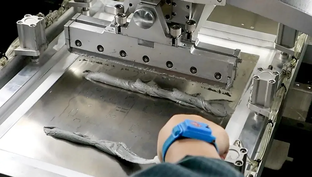
Common Defects in the Solder Paste Printing Process
The solder paste printing stage deposits the exact volume of solder alloy onto PCB pads. Variations here directly affect joint formation and account for up to 30% of all SMT assembly defects.
Solder Bridges
Solder bridges occur when excess paste connects adjacent pads, creating unintended short circuits. Primary causes include over-pressured printing, worn or clogged stencil apertures, and high-viscosity paste that fails to release cleanly. In fine-pitch components (0.4 mm or less), bridges can raise defect rates by 5–10% and trigger immediate electrical failures during testing.
Open Circuits / Insufficient Solder
Open circuits or insufficient solder result when too little paste is deposited, leaving pads without adequate material for a reliable joint. This stems from clogged stencil apertures, uneven squeegee pressure, or paste slump during printing. The defect produces open connections that fail IPC-A-610H Class 3 criteria and often require full board rework, reducing throughput in high-volume lines.
Precision Challenges in the Component Placement Phase
Automated pick-and-place machines position thousands of components per hour, but mechanical and programming inaccuracies introduce placement-related SMT defects that propagate into reflow.
Component Misalignment
Misalignment happens when components are offset from pad centers due to vision system calibration drift, nozzle wear, or incorrect feeder setup. Offsets as small as 0.05 mm can cause tombstoning or poor wetting later, especially on 0201 and 01005 packages.
Component Shift
Component shift occurs post-placement but pre-reflow, caused by vibration, paste tackiness variation, or conveyor movement. Shifted parts create skewed joints that fail mechanical strength tests and increase field failure risk under thermal cycling.
Component Damaged
Damaged components result from excessive nozzle pressure, incorrect vacuum levels, or collisions during high-speed placement. Cracked capacitors or bent leads lead to immediate rejection or latent failures, emphasizing the need for precise force control in modern chip-shooter systems.
Related Reading: Troubleshooting Component Misalignment in PCB Manufacturing: A Practical Guide
Thermal-Induced Defects During Reflow Soldering
The reflow stage melts the solder paste to form permanent joints. Thermal imbalances here generate some of the most visually dramatic SMT defects.
Tombstoning / Manhattan Effect
One end of a passive component lifts vertically due to uneven heating or mismatched thermal mass on the two pads. This is common with 0402 and 0201 chips when one side reaches liquidus temperature faster.
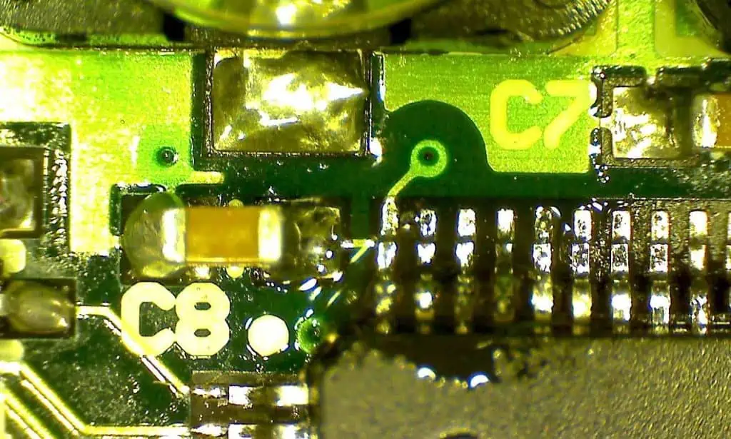
Solder Balls
Small spherical solder droplets form when flux volatiles escape too rapidly or paste is contaminated. They create potential shorts and cosmetic failures that fail IPC-A-610H inspection.
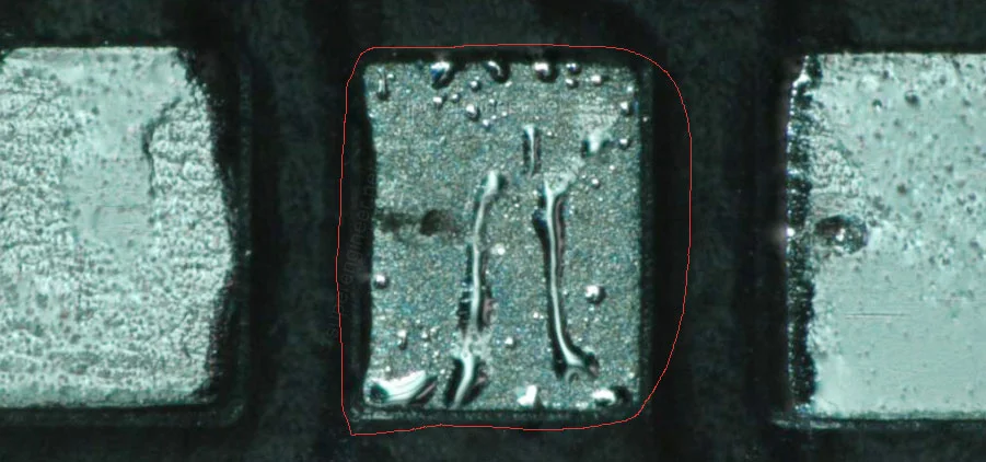
Solder Voids
Trapped gas or flux residue creates internal voids within the joint, reducing mechanical strength by up to 40% and increasing thermal resistance—critical in power electronics.
De-wetting / Non-wetting
Molten solder fails to spread or retracts from surfaces due to oxidation, poor flux activity, or incompatible surface finishes. Exposed copper or leads result in weak, unreliable connections.
Lifted Leads
Component leads lift from pads during cooling due to CTE mismatch or excessive thermal stress. This defect is prevalent in QFP and SOIC packages and compromises both electrical and mechanical integrity.
Related Reading: Troubleshooting Common Reflow Oven Problems: A Practical Guide for Electronics Manufacturers
Summary of Common SMT Defects
| Defect | Workflow Stage | Primary Cause | Typical Impact | IPC Standard Reference |
|---|---|---|---|---|
| Solder Bridges | Paste Printing | Excess paste / stencil issues | Short circuits | IPC-A-610H Class 2/3 |
| Open Circuits / Insufficient Solder | Paste Printing | Insufficient volume / clogging | Open connections | IPC-A-610H |
| Component Misalignment | Placement | Vision / nozzle error | Skewed joints | IPC-A-610H |
| Component Shift | Placement | Vibration / paste tackiness | Misplaced parts post-reflow | IPC-A-610H |
| Component Damaged | Placement | Excessive force / collision | Cracked parts, latent failures | IPC-A-610H |
| Tombstoning | Reflow | Uneven heating | Lifted components | IPC-A-610H |
| Solder Balls | Reflow | Flux outgassing / contamination | Potential shorts | IPC-A-610H |
| Solder Voids | Reflow | Trapped gas | Reduced strength & thermal issues | IPC-A-610H |
| De-wetting / Non-wetting | Reflow | Oxidation / poor flux | Weak or exposed joints | IPC-A-610H |
| Lifted Leads | Reflow | CTE mismatch / stress | Open or intermittent connections | IPC-A-610H |
Related Reading: Common Soldering Defects and Their Impact on PCB Reliability
Practical Solutions to Prevent SMT Defects
Design for Manufacturability (DFM) Optimization
Early DFM reviews ensure pad sizes, stencil apertures, and component spacing follow IPC-7351B recommendations. Collaborative design-assembly reviews can reduce SMT defects by 20–30% before production begins.
Solder Paste Management & Stencil Design
Use laser-cut stencils with electropolished apertures, control paste temperature (22–26°C), and implement regular stencil cleaning cycles. Advanced nano-coatings and step-stencil designs improve release for fine-pitch applications.
Automated Inspection (SPI & AOI)
Inline Solder Paste Inspection (SPI) catches volume and alignment issues immediately after printing, while Automated Optical Inspection (AOI) and X-ray systems verify post-reflow joints. These tools enable real-time smt assembly workflow troubleshooting and reduce escaped defects by over 90%.
Thermal Profiling and Reflow Calibration
Develop board-specific profiles using thermocouples at multiple locations, ensuring peak temperatures stay within solder alloy tolerances (typically 235–245°C for SAC305). Regular oven calibration and nitrogen atmosphere options minimize oxidation-related SMT defects.
Related Reading: Prevent SMT Soldering Defects: Tips
Conclusion
SMT assembly defects across the paste printing, component placement, and reflow stages pose persistent challenges to electronics manufacturers. By understanding their root causes—from stencil issues and placement inaccuracies to thermal imbalances—engineers can implement targeted smt assembly workflow troubleshooting and prevention measures. Optimizing DFM, paste management, automated inspection, and reflow profiling dramatically reduces defect rates, improves first-pass yield, and ensures reliable performance in demanding applications. Proactive adherence to IPC standards transforms potential failures into predictable, high-quality outcomes.
FAQs
Q1: What causes Empty Solder or Missing Solder in SMT assembly?
A1: Insufficient paste volume from stencil clogging or misalignment during printing, combined with poor reflow. Regular stencil maintenance and SPI inspection prevent this common SMT defect.
Q2: How can Cold Solder joints be identified and fixed?
A2: They appear dull and grainy due to insufficient heat. Visual or X-ray inspection identifies them; controlled re-reflow resolves the issue while proper thermal profiling prevents recurrence.
Q3: Why does poor Wetting occur in SMT PCB assembly?
A3: Surface contamination or inadequate flux prevents solder spread. Clean storage, effective flux, and optimized reflow profiles restore proper wetting.
Q4: How do industry standards help prevent SMT assembly defects?
A4: Standards like IPC-A-610H and IPC J-STD-001H define acceptance criteria and best practices for each workflow stage, enabling consistent quality and effective smt assembly workflow troubleshooting.
References
IPC-A-610H — Acceptability of Electronic Assemblies. IPC, 2021.
IPC J-STD-001H — Requirements for Soldered Electrical and Electronic Assemblies. IPC, 2021.
IPC-A-600K — Acceptability of Printed Boards. IPC, 2020.
IPC J-STD-020E — Moisture/Reflow Sensitivity Classification. JEDEC, 2014.


