Introduction
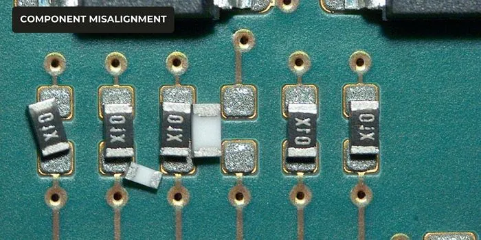
Component misalignment in PCB manufacturing poses significant challenges during surface mount technology assembly processes. Electrical engineers often encounter issues where components shift, rotate, or deviate from their intended positions, leading to assembly defects and reduced product reliability. Understanding PCB misalignment causes helps in implementing targeted troubleshooting strategies that maintain high yields and performance standards. This guide provides practical insights into identifying root causes, applying preventive measures, and correcting placement defects effectively. By focusing on key stages like stencil printing, component placement, and reflow soldering, engineers can optimize their manufacturing workflows.
Why Component Misalignment Matters in PCB Manufacturing
Component misalignment directly affects electrical connectivity, signal integrity, and overall board functionality in electronic assemblies. Even minor deviations can result in open circuits, solder bridges, or intermittent failures that compromise high-speed designs. In production environments, these defects increase rework costs and delay time-to-market for critical applications. According to industry benchmarks, preventing component rotation and shift during soldering is essential for meeting quality requirements in class 2 and class 3 assemblies. Engineers must prioritize alignment accuracy to ensure compliance with standards like IPC-A-610J, which defines acceptability criteria for electronic assemblies. Addressing these issues upfront enhances yield rates and supports scalable manufacturing.
Common PCB Misalignment Causes
Several factors contribute to PCB misalignment causes across the SMT process. During stencil printing, excessive squeegee pressure or poor stencil tension can cause solder paste misalignment, depositing uneven volumes that lead to component drift later. PCB warpage from uneven copper distribution or improper baking exacerbates this by creating non-planar surfaces that challenge placement heads. Machine-related issues, such as worn nozzles or inadequate vision system calibration, further introduce offsets in pick-and-place operations.
Component shift during soldering often stems from reflow oven dynamics. Imbalanced surface tension forces in molten solder paste pull components off-center, especially for small passives like 0201 resistors. Gas turbulence from rapid heating or conveyor vibrations can amplify this shift, pushing parts beyond pad boundaries. Preventing component rotation requires attention to pad geometry mismatches, where asymmetric thermal masses cause uneven wetting during reflow.
Design and material factors also play roles in misalignment. Fiducial mark inconsistencies or tolerances in panelization lead to repeatable offsets across batches. Bent leads on components or dimensional variations from suppliers introduce initial inaccuracies that propagate through assembly.
Technical Mechanisms Behind Misalignment
The physics of SMT assembly reveals precise mechanisms driving these defects. In placement, accuracy depends on machine repeatability, quantified by standards like IPC-9850A for surface mount placement equipment characterization. Vision systems align fiducials to achieve sub-50-micron precision, but environmental factors like temperature fluctuations alter nozzle heights and board positions.
During reflow, solder paste transitions from solid to liquid, generating capillary forces that self-align components if paste volume is optimal. Excessive paste leads to floating, while insufficient amounts cause tombstoning or rotation due to unbalanced torques. Component shift during soldering occurs when preheat rates exceed paste activation thresholds, creating volatile gases that propel parts.
Rotation specifically arises from asymmetric pad wetting, where one side of a component melts faster, generating torque. Engineers can model this using thermal profiles to predict behavior. IPC J-STD-001J outlines requirements for soldered assemblies, emphasizing controlled profiles to minimize these effects.
Practical Solutions for Preventing Misalignment
Implementing best practices starts with design for manufacturability. Ensure fiducials are symmetrically placed with at least 1 mm clearance from edges and metals, enabling precise board registration. Balance copper layers to minimize warpage below 0.75% for standard panels, verified through shadow moiré testing.
Stencil design is critical for solder paste deposition. Use laser-cut stencils with 5-10 micron tolerances and apertures sized to 100-120% of component width for optimal volume. Print parameters like 1.5-2.0 kg squeegee pressure and 45-degree angles prevent smearing.
Calibrate pick-and-place machines regularly per IPC-9850A guidelines, targeting 2-sigma placement accuracy under 50 microns. Employ dual-head systems with height sensors for warped boards. For preventing component rotation, verify component orientation in feeders and use nozzles matched to part sizes.
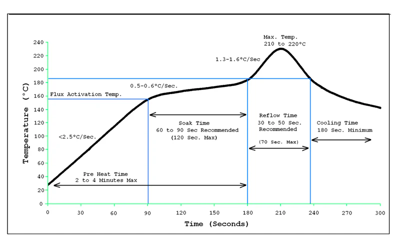
Optimize reflow profiles with linear ramps: 1-2°C/s preheat, peak at 245-260°C for lead-free, and cool at 2-4°C/s. This controls viscosity and minimizes shift. Post-print inspection via SPI confirms paste alignment before placement.
Troubleshooting and Correcting Placement Defects
When defects occur, systematic troubleshooting isolates root causes. Begin with AOI or X-ray inspection to quantify offsets, distinguishing placement errors from reflow shifts. Measure against IPC-A-610J criteria, where deviations over 25% pad width for class 3 assemblies require rework.
For PCB misalignment causes traced to printing, clean stencils and adjust gaskets. Component shift during soldering demands profile tweaks or paste reformulation for better cohesion. Preventing component rotation involves pad redesign for symmetry if recurrent.
Rework techniques include hot air stations for desoldering shifted parts, followed by precise re-placement. Use flux and minimal heat to avoid pad damage. Validate corrections with flying probe testing for continuity.
A common case involves high-density boards where warpage caused 5% shift rates. Baking panels at 125°C for 4 hours, combined with vacuum fixturing, reduced defects to under 0.5%. Document process capability indices (Cpk >1.33) for ongoing monitoring.
Conclusion
Troubleshooting component misalignment demands a holistic approach from design to inspection. By addressing PCB misalignment causes like warpage, paste issues, and reflow dynamics, engineers achieve robust assemblies. Adopting standards such as IPC-9850A, IPC J-STD-001J, and IPC-A-610J ensures consistent quality. Practical steps like fiducial optimization, machine calibration, and profile control directly prevent component shift during soldering and rotation. Correcting placement defects through targeted rework minimizes downtime. Ultimately, these strategies enhance reliability for demanding electrical engineering applications.
FAQs
Q1: What are the primary PCB misalignment causes in SMT assembly?
A1: PCB misalignment causes include stencil printing inaccuracies, placement machine offsets, PCB warpage, and reflow-induced shifts. Vibrations, uneven paste deposition, and fiducial errors contribute significantly. Addressing these through calibration and design reviews prevents most issues. Regular SPI checks help detect early.
Q2: How can I prevent component shift during soldering?
A2: Prevent component shift during soldering by optimizing reflow profiles with controlled ramp rates and peak temperatures per IPC J-STD-001J. Ensure solder paste volume matches pad geometry to leverage surface tension for self-alignment. Use low-voiding pastes and minimize conveyor speeds. Baking boards reduces moisture-related turbulence.
Q3: What techniques stop component rotation in PCB manufacturing?
A3: Preventing component rotation involves symmetric pad designs and balanced thermal masses to avoid uneven wetting. Calibrate placement machines for angular accuracy using IPC-9850A methods. Verify feeder orientations and use vision confirmation. Post-placement stabilization before reflow further secures parts.
Q4: How do I correct placement defects after assembly?
A4: Correcting placement defects starts with AOI identification against IPC-A-610J criteria. Rework shifted components via selective soldering or hot air, then inspect joints. Analyze root causes like warpage for prevention. Process audits ensure recurrence rates stay low.
References
IPC-9850A — Surface Mount Placement Equipment Characterization. IPC, 2011
IPC J-STD-001J — Requirements for Soldered Electrical and Electronic Assemblies. IPC, 2024
IPC-A-610J — Acceptability of Electronic Assemblies. IPC, 2024


