Introduction
Solder joint quality directly impacts the reliability and performance of printed circuit boards in electronic assemblies. Defects such as voids, cracks, or insufficient wetting can lead to failures in the field, making effective inspection critical during PCB manufacturing. Automated Optical Inspection (AOI) and X-ray inspection stand out as primary techniques for solder joint evaluation, each offering unique capabilities suited to different assembly complexities. This article compares AOI solder joint inspection and X-ray solder joint inspection, helping engineers select the optimal method based on component types, production volume, and defect risks. Understanding the solder joint inspection comparison ensures compliance with quality standards and minimizes rework costs. Factory teams rely on these PCB inspection techniques to achieve high yields and long-term board functionality.
What Is AOI Solder Joint Inspection and Why Does It Matter?
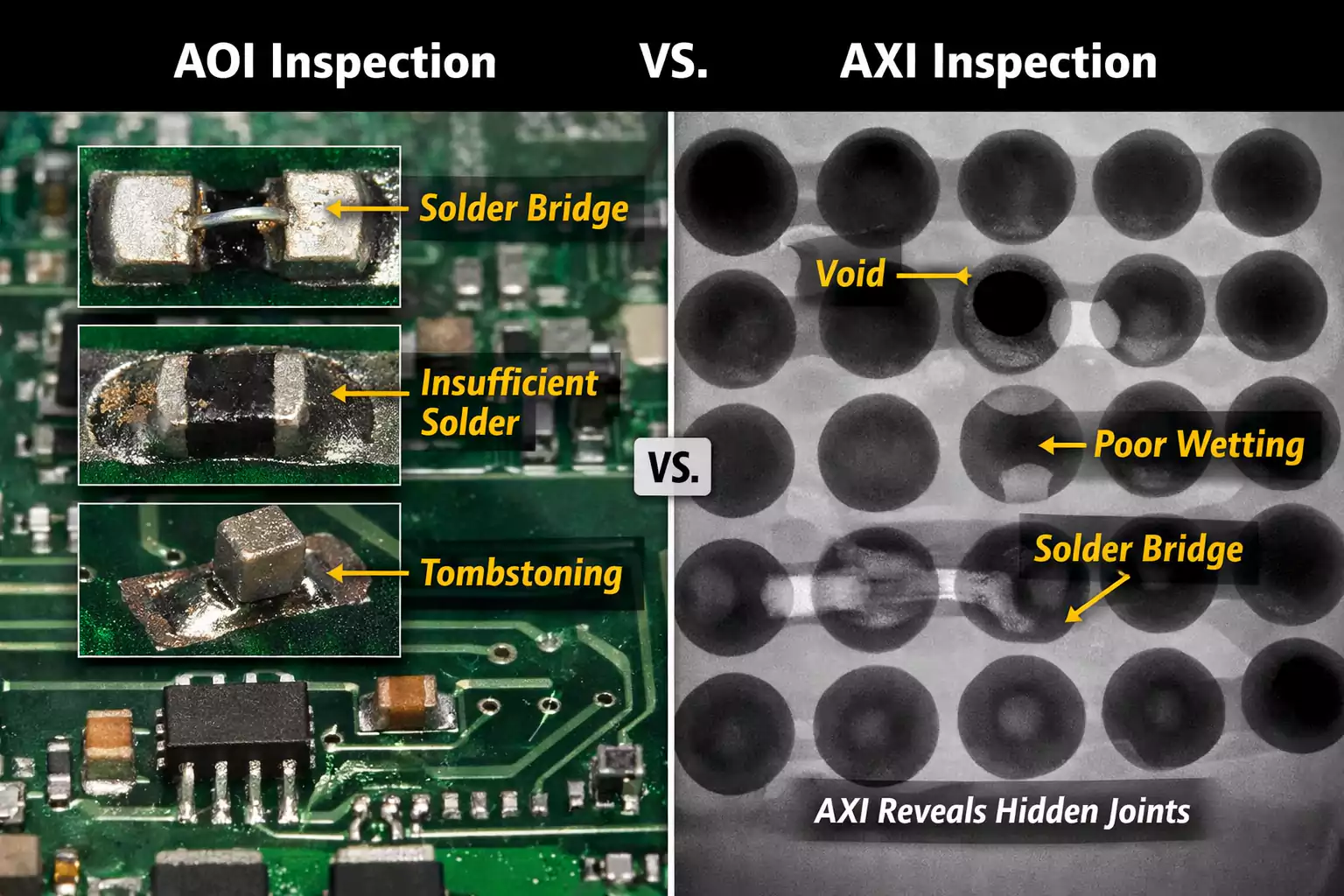
AOI solder joint inspection uses high-resolution cameras and structured lighting to capture 2D images of PCB surfaces in real time. Algorithms analyze these images against predefined golden samples or CAD data to detect visible anomalies like bridging, missing solder, tombstoning, or component misalignment. This method excels in high-volume surface-mount technology (SMT) lines where speed is essential, typically inspecting hundreds of boards per hour. In manufacturing environments, AOI provides immediate feedback, allowing operators to halt production for corrections before defects propagate. Its relevance grows with the prevalence of fine-pitch components, where manual inspection proves inadequate for consistency. According to IPC-A-610, acceptability criteria for solder joints emphasize uniform fillet shapes and wetting, which AOI effectively verifies on exposed joints.
AOI matters because it integrates seamlessly into assembly lines, reducing escape defects to post-reflow processes. Engineers appreciate its non-contact nature, which avoids handling sensitive boards. Limitations arise with obscured joints, but for accessible pads, it delivers cost-effective quality control. Factories often deploy multiple AOI stations for pre- and post-reflow checks, enhancing overall process control.
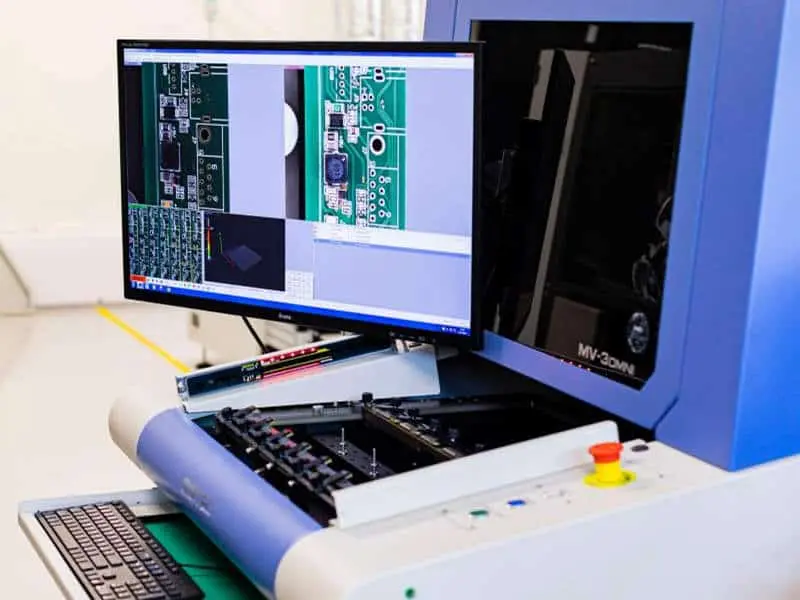
What Is X-Ray Solder Joint Inspection and Its Industry Role?
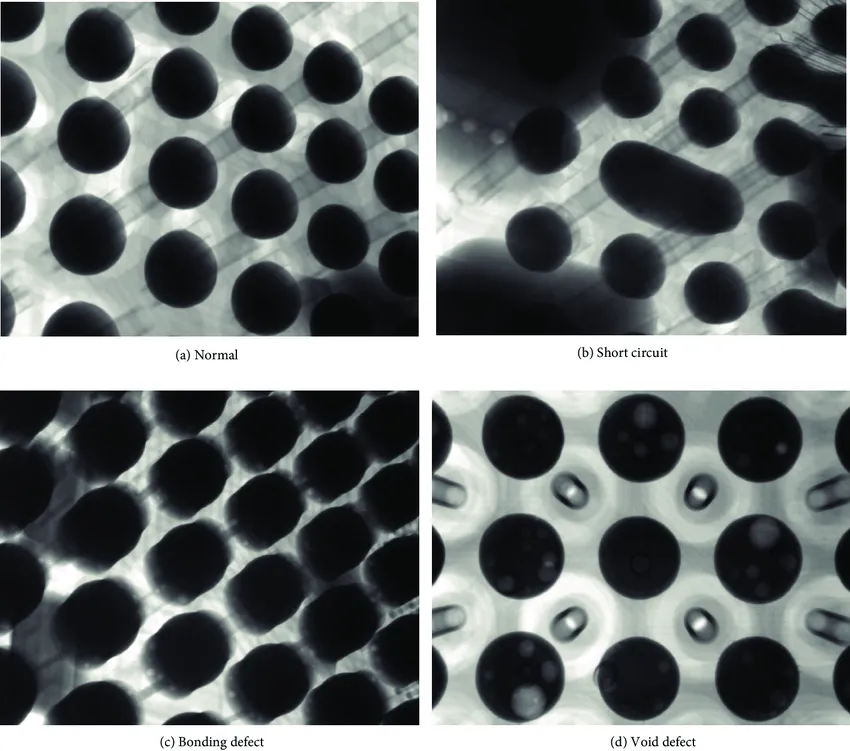
X-ray solder joint inspection employs ionizing radiation to penetrate components and reveal internal structures invisible to optical methods. Transmission X-ray systems project shadows of solder joints onto detectors, highlighting issues like voids, head-in-pillow defects, or ball grid array (BGA) misalignment. Oblique-angle or 3D computed tomography variants provide layered views for precise void percentage measurements. This technique proves indispensable for bottom-terminated components such as quad flat no-leads (QFNs), BGAs, and chip-scale packages where joints hide beneath package bodies. In high-reliability sectors, X-ray ensures joints meet mechanical stress requirements under thermal cycling.
The role of X-ray in PCB inspection techniques underscores its value for complex assemblies with double-sided populations or cavity-down packages. Production teams use it sparingly due to cycle times of seconds per board, reserving it for targeted sampling or failure analysis. Its density-sensitive imaging distinguishes solder from base materials accurately. Compliance with J-STD-001 requirements for joint integrity benefits from X-ray's subsurface insights, preventing latent failures.
Technical Principles of AOI and X-Ray in Solder Joint Evaluation
AOI operates on photometric principles, where multi-angle LED illumination creates shadows and highlights to model 3D features from 2D images. Phase-shift algorithms reconstruct height profiles for solder volume estimation, comparing against tolerance bands derived from design rules. Color segmentation isolates joints from pads, while machine learning refines defect classification over time. This approach suits symmetric defects but struggles with specular reflections on shiny solder surfaces.
X-ray principles rely on differential absorption, where solder's high atomic number attenuates low-energy X-rays more than silicon or copper. Detectors convert transmitted photons into grayscale images, with voids appearing as lighter regions due to reduced mass. Automated analysis thresholds grayscale values to quantify fill factors, often calibrated to detect voids exceeding 25% of joint area. Tilted imaging compensates for parallax in stacked components.
Both methods align with IPC standards for defect categorization, but their resolutions differ: AOI at sub-micron pixel levels for surfaces, X-ray at 1-5 microns for internals. Engineers must consider radiation safety protocols for X-ray, including shielding and dosimetry.
AOI vs. X-Ray PCB Inspection: A Detailed Comparison
- Visibility: AOI — Surface-level only; X-ray — Subsurface and hidden joints.
- Speed: AOI — High (milliseconds per joint); X-ray — Moderate (seconds per board).
- Resolution: AOI — Optical (2-10 μm); X-ray — Radiographic (1-5 μm).
- Cost: AOI — Lower initial and operating; X-ray — Higher due to equipment and maintenance.
- Common defects detected: AOI — Bridges, insufficient solder, misalignment; X-ray — Voids, cracks, BGA offset.
- Best for: AOI — High-volume SMT, pre-reflow; X-ray — Low-volume, high-density BGAs.
This solder joint inspection comparison highlights complementary strengths. AOI dominates in detecting polarity errors and paste volume issues early, while PCB X-ray inspection excels in post-reflow validation of fillet formation under packages. Factories balance throughput by using AOI inline and X-ray offline.
Advantages and Limitations in Manufacturing Contexts
AOI's advantages include rapid programming via Gerber files and high uptime in automated lines, making it ideal for just-in-time production. It flags process drifts like stencil wear through statistical process control integration. However, false calls from lighting variations or dirt require operator verification, and it misses intermetallic growth over time.
X-ray advantages lie in quantitative metrics, such as void distribution histograms, aiding root cause analysis per IPC guidelines. Its non-destructive nature supports 100% inspection of critical boards. Drawbacks encompass image artifacts from multi-layer boards and the need for skilled interpretation of halation effects.
In practice, AOI handles 90% of routine checks, with X-ray intervening for risk-based sampling.
Best Practices for Choosing Your Solder Joint Inspection System
Choose AOI for assemblies with leaded or visible SMT joints, prioritizing line speed above subsurface detail. Program AOI with multiple thresholds to minimize nuisance alarms, and validate against known good boards. Integrate it post-printing, post-reflow, and pre-conformal coating for layered assurance. Proper stencil design directly impacts paste volume and subsequent solder joint quality—see our guide on optimizing solder paste stencil design.
Opt for X-ray when BGA pitch falls below 0.5 mm or when thermal reliability demands void minimization. Employ 3D X-ray for volume rendering in prototyping phases. Combine techniques in hybrid flows: AOI first for gross defects, X-ray for sampled high-risk zones.
Calibrate systems regularly per manufacturer specs, and train teams on defect taxonomy from IPC-A-610. Document inspection data for traceability in quality audits.
Case Insights: Real-World Application in High-Density Assemblies
In a factory producing telecom modules with mixed QFN and BGA footprints, AOI caught 95% of surface bridges during ramp-up, but X-ray revealed 15% void rates in QFNs missed optically. Switching to oblique X-ray reduced escapes by confirming joint symmetry. Engineers adjusted reflow profiles based on X-ray data, aligning with J-STD-001 void limits.
Troubleshooting tip: For intermittent failures, correlate AOI misses with X-ray cross-sections to identify hidden cracks from board flexure.
Conclusion
Selecting between AOI and X-ray hinges on joint visibility, production scale, and reliability needs in PCB inspection techniques. AOI delivers efficient surface scrutiny for volume manufacturing, while X-ray provides essential subsurface validation for advanced packages. A strategic blend maximizes defect detection without bottlenecks. Engineers benefit from standard-driven criteria to guide decisions, ensuring robust solder joints. Implementing these methods elevates assembly quality and supports scalable operations.
FAQs
Q1: What are the main differences in AOI vs. X-ray PCB inspection for solder joints?
A1: AOI solder joint inspection focuses on 2D optical imaging for visible defects like bridges and misalignment, offering high speed for inline use. X-ray solder joint inspection penetrates components to detect voids and cracks in hidden areas such as BGAs. AOI suits high-volume lines, while X-ray excels in detailed analysis of dense packages. Factories often pair them for complete coverage, balancing cost and thoroughness.
Q2: When should electric engineers prefer AOI solder joint inspection over X-ray?
A2: Choose AOI for accessible SMT joints in mass production, where rapid detection of paste issues and component placement errors is key. It integrates easily into reflow lines per IPC guidelines, minimizing downtime. Reserve X-ray for prototypes or failure analysis. This solder joint inspection comparison favors AOI when subsurface risks are low and throughput is priority.
Q3: Can X-ray replace AOI in PCB inspection techniques entirely?
A3: No, X-ray cannot fully replace AOI due to slower speeds and higher costs, making it impractical for 100% high-volume checks. AOI handles surface defects efficiently, complementing X-ray's strength in BGA voids. Best practices involve sequential use: AOI first, X-ray for confirmation. This approach aligns with manufacturing efficiency standards.
Q4: How do standards influence AOI vs. X-ray solder joint inspection choices?
A4: Standards like IPC-A-610 define joint acceptability, guiding AOI for fillet visuals and X-ray for internal voids per J-STD-001. Engineers reference them to set thresholds, ensuring compliance. In comparisons, standards highlight AOI's role in visible criteria and X-ray's in hidden integrity. Factory decisions prioritize these for reliable outcomes.
References
IPC-A-610H — Acceptability of Electronic Assemblies. IPC, 2019
J-STD-001H — Requirements for Soldered Electrical and Electronic Assemblies. IPC/JEDEC, 2020


