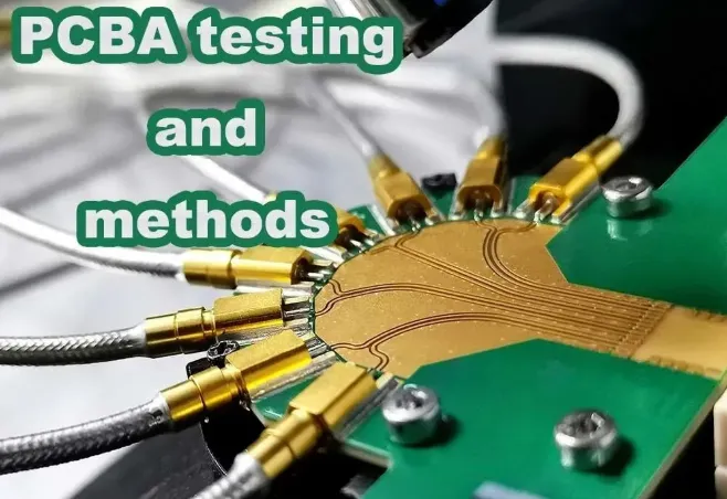
Printed circuit boards (PCBs) and PCB assemblies (PCBA) are used across electronic devices from smartphones and computers to complex machinery. Defects in a PCB or PCBA can cause product failures, recalls, and increased time and cost to repair. Testing PCBA during manufacturing is therefore essential to detect issues early, assist troubleshooting, and maintain product quality.
Below are 14 commonly used PCB and PCBA test methods.
1. In-Circuit Test (ICT)
In-circuit test (ICT) is an automated testing method widely used in PCB manufacturing. It uses test probes to contact PCB test points to check circuit continuity, short circuits, and component faults, and reports specific failure locations to technicians. ICT provides high measurement accuracy and clear fault indication, which helps operators identify and fix defective PCBA quickly. Using ICT can improve production efficiency and reduce manufacturing costs.
2. Flying Probe Test
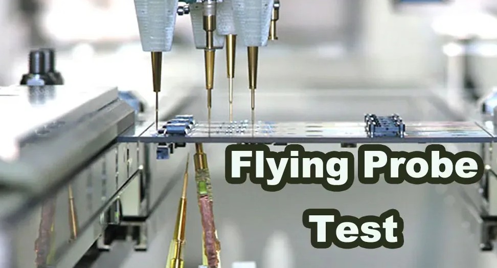
Flying probe test and ICT are both effective for detecting production quality issues. Flying probe testing uses two or more independent probes that move under program control rather than relying on a fixed fixture. Its lower initial fixture cost and flexibility make it cost-effective for small production batches because it can be reprogrammed without changing hardware. ICT, however, has higher initial fixture cost but is faster and less error-prone for high-volume production.
3. Functional Test
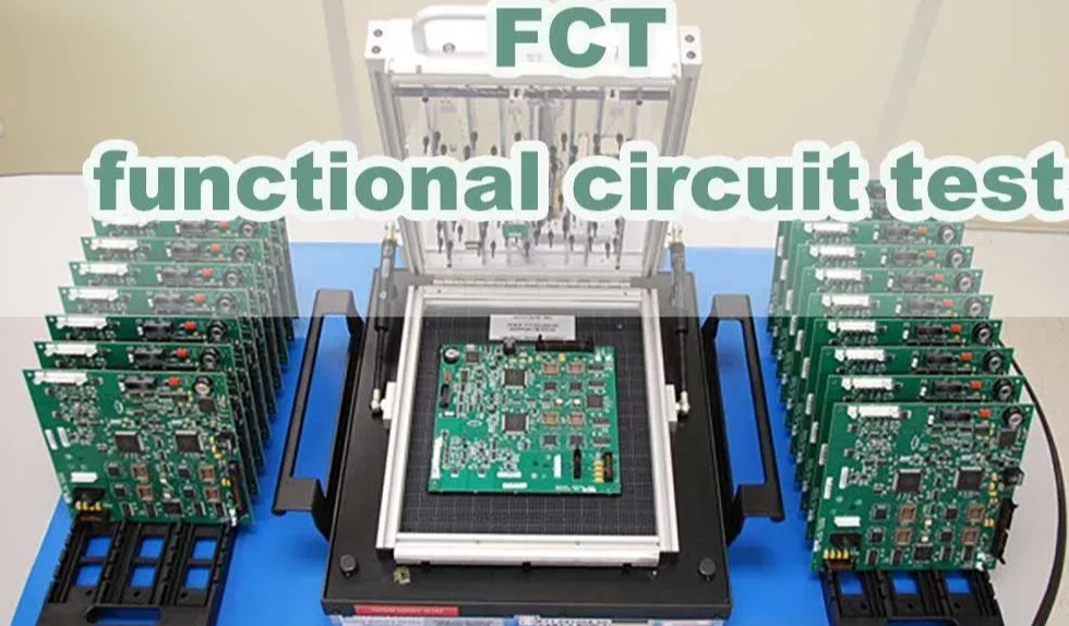
Functional testing uses dedicated test equipment at mid-line or end-of-line to exercise the board's functional modules and confirm overall quality. Functional tests include final product tests and hot mock-ups. These tests typically do not provide detailed component-level diagnostics such as pin-level faults and therefore require specially designed equipment and complex test programs. Writing functional test programs is complex, so functional testing is not suitable for all production lines.
4. Automated Optical Inspection (AOI)
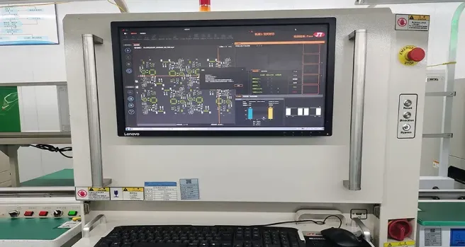
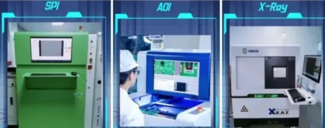
AOI captures images of a PCB using a 2D camera or dual 3D cameras, then compares the photos to detailed schematics. Discrepancies are flagged for technician review. AOI does not power the board, so it cannot detect all component failures by itself. AOI is commonly combined with other test methods, such as:
- AOI plus flying probe
- AOI plus ICT
- AOI plus functional test
5. X-ray Inspection
X-ray inspection uses low-energy X-rays to detect open circuits, shorts, voids, and soldering defects quickly. It is especially useful for ultra-fine pitch and high-density boards and for identifying bridging, missing chips, and misalignment introduced during assembly. X-ray computed tomography can also reveal internal defects within IC packages. X-ray is the only practical method to inspect ball grid array (BGA) solder joints and embedded components without specific fixtures.
6. Laser Inspection
Laser inspection scans the board with a laser beam to collect dimensional and positional measurements and compares the results to acceptance limits. The technique has been validated for bare boards and is under consideration for assembled board testing. Laser inspection offers fast output, no fixtures, and good visual access; its drawbacks include higher initial cost and maintenance considerations.
7. Burn-In (Aging) Test
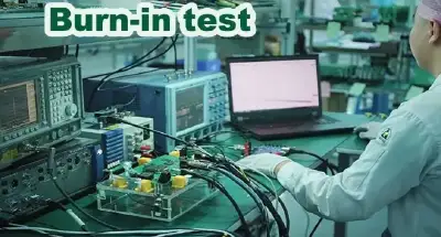
Burn-in testing subjects products to stress conditions that simulate extended use, such as elevated temperature and humidity, to evaluate stability and reliability under specified environmental conditions. Typical procedures run continuously for 72 hours to 7 days while recording performance data to identify and correct manufacturing issues. Related reliability tests include drop, vibration, and salt spray testing.
8. Solderability Test
Solderability testing evaluates the ability of a surface to form a reliable solder joint. Using the wetting balance method, solderability tests provide qualitative and quantitative assessment of components, PCB pads, solder alloys, and flux behavior.
9. PCB Contamination Test
PCB contamination refers to ionic residues from flux, cleaning agents, humidity exposure, plating, wave soldering, reflow soldering, and other processes. Conductive or corrosive ionic residues on the PCBA surface can lead to corrosion and functional failures. Contamination tests measure ionic contamination levels to identify process issues.
10. Cross-Section (Slice) Analysis
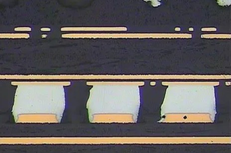
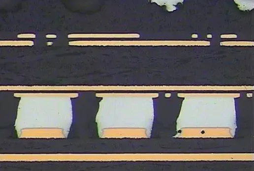
Cross-section analysis investigates defects, opens, shorts, and other failure modes by cutting and preparing board or component cross sections for microscopic inspection. This method is useful for root-cause analysis and metallurgical evaluation.
11. Time Domain Reflectometry (TDR)
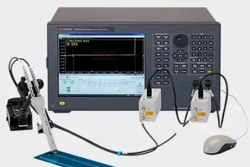
TDR is recommended for diagnosing faults on high-speed or high-frequency boards. It can quickly detect opens and shorts and locate the fault position along a trace using reflected signal analysis.
12. Peel Strength Test
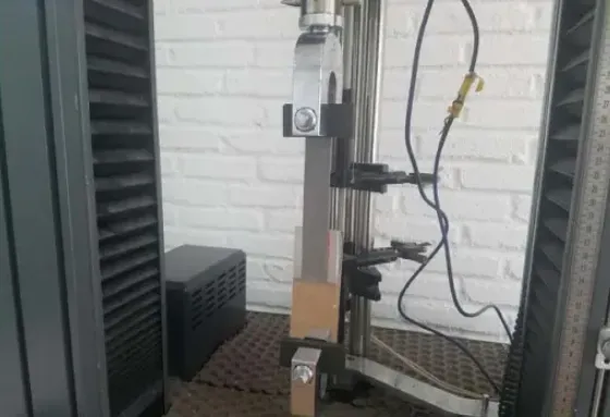
Peel strength testing measures the bond strength between copper foil and the substrate or between copper foil and sealant films. The test evaluates the bond under as-received conditions, after thermal stress, and at elevated temperatures to ensure adhesion meets design requirements.
13. Solder Float Test
Solder float testing assesses the thermal resistance of plated through-holes, surface conductors, and pads. Before testing, flux residues and dross must be removed. The sample is immersed into molten solder for up to 5 minutes with immersion depth not exceeding 50% of the sample thickness. After immersion, the sample is removed and allowed to cool horizontally until the solder solidifies.
14. Wave Solder Test
Wave solder testing applies to plated through-holes, surface conductors, and pads. Relevant parameters such as fixture method, conveyor speed, preheat profile, use of anti-oxidation agents, process controls, tilt angles, board preheat temperature, and solder temperature should be set and recorded.
PCBA testing is a critical part of ensuring delivered product quality. Proper test planning and implementation determine product performance, control quality, and reduce after-sales failures and repair rates.