










Introduction
Have you ever struggled to find a specific component during PCB layout, or spent time rearranging dense parts just to improve the placement? This article summarizes two practical techniques—interactive layout and modular layout—that can significantly speed up component placement and make your PCB design more organized.
Interactive Layout: Schematic and PCB in Sync
"See to select, select to sync" captures the essence of interactive layout.
Enable Cross Select Mode so that when you click a component in the schematic it highlights on the PCB, and vice versa. This eliminates back-and-forth searching and lets you locate components with a single action.
How to enable interactive mode
- In the schematic interface, open the menu and select
Tools > Cross Select Mode.
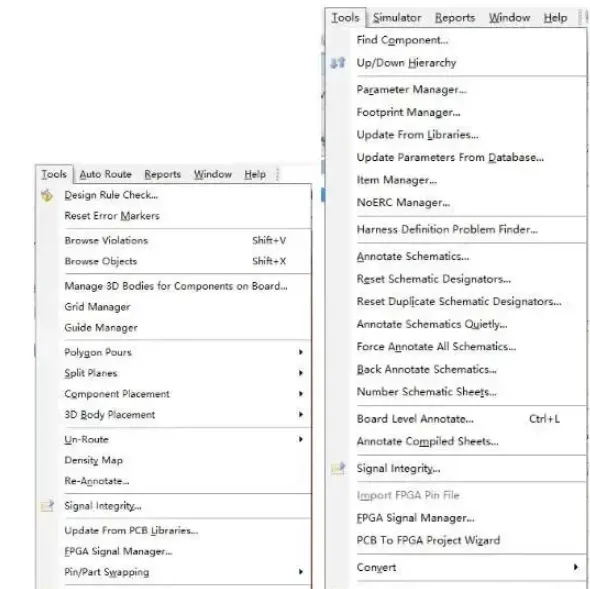
2. In the PCB interface, perform the same operation to enable the mode there as well.
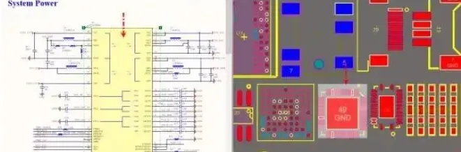
Once enabled, selecting any component in one view immediately highlights the corresponding item in the other view, which can double placement efficiency.
Modular Layout: Organize Components by Function
If you want components that belong to the same functional block to be grouped and easy to find, modular layout helps achieve that.
One useful feature is Arrange Components Inside Area. It arranges the selected components neatly inside a defined rectangular area, which is especially helpful for quickly defining module regions in the early layout stage.
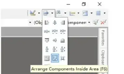
Steps
Select the module: In the schematic, use interactive selection to box a functional module.
PCB sync: The corresponding components are automatically selected in the PCB view.
Arrange neatly: Use the Arrange Components tool to position the components inside the target area.
Fine-tune placement: Adjust placement for ICs, resistors, capacitors, and other parts for routing and performance considerations.
The result is a PCB where functional modules are orderly, improving both layout clarity and routing efficiency.
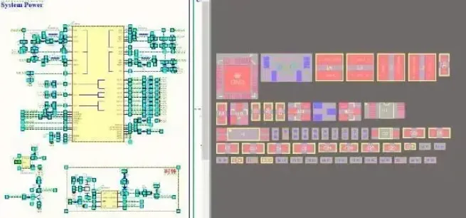
Tip
Use Split Vertical to show the schematic and PCB side by side. Selecting in one view while observing placement in the other makes the workflow more intuitive.
Design is not afraid of complexity, but of disorder. Using the appropriate tools improves efficiency.






