










In low-voltage, high-current designs, 1 mΩ is not negligible: at 100 A it corresponds to a 0.1 V drop and 10 W of loss. With irregular copper pours, narrow necks, multilayer transitions and via farms, it's difficult to judge true resistance and current distribution by visual inspection alone.
Fill Resistance, developed by KiCad community contributor Janik Oltmanns, addresses this problem. In the author's words: "How many milliohms does this copper pour actually have?"
The plugin reads the copper pours, traces, pads and vias of a specified net in a KiCad PCB, solves the potential field across one or more copper layers, then computes total resistance, voltage drop, power loss, current density and the current through each via. The latest release also adds a PDN mode that can model multiple power sources and multiple loads on the same power network.
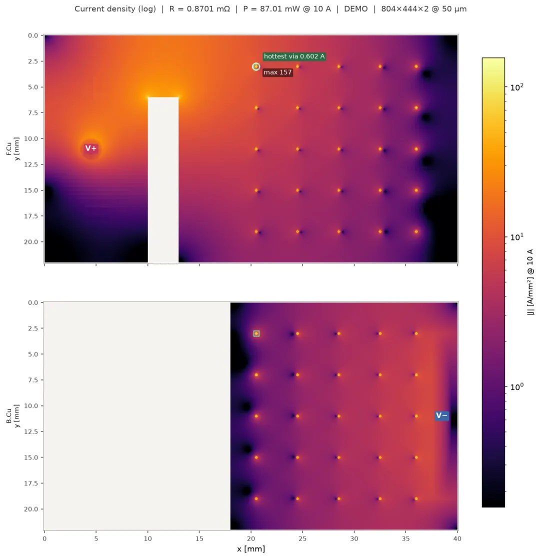
Example current density map: the plugin highlights current-crowded regions and the via carrying the highest current.
Not just "calculate trace resistance"
Conventional copper-resistance estimates start from length, width, copper thickness and resistivity, but real PCB current paths rarely form a regular rectangle. Current redistributes around corners, slots, connector pads, MOSFET arrays and via arrays, often producing significant current crowding.
Classic mode: three steps to reveal copper pour IR drop and currents
-
Define current injection and extraction points
You can select two pads or vias directly. When one side includes multiple contact points, draw rectangles on user layers (for example,
User.1andUser.2) to group multiple pads, plated through-holes or contact regions into V+ and V? sets.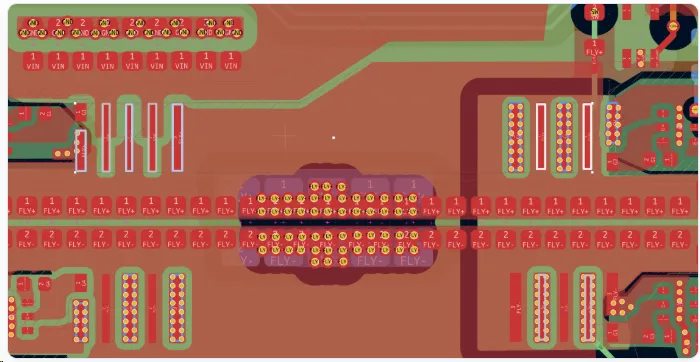
In power boards, use user-layer rectangles to mark groups of FET pads belonging to positive and negative contact sets.
-
Click the Ω toolbar button and set solver parameters
In the dialog choose the net, the copper layers to include, the test current, grid size and the contact model. Multilayer copper pours are coupled via vias and plated through-hole pads that belong to the same net. The frequency field can be filled to estimate additional resistance from skin effect, but this is only an approximate correction and does not represent a complete AC impedance analysis.
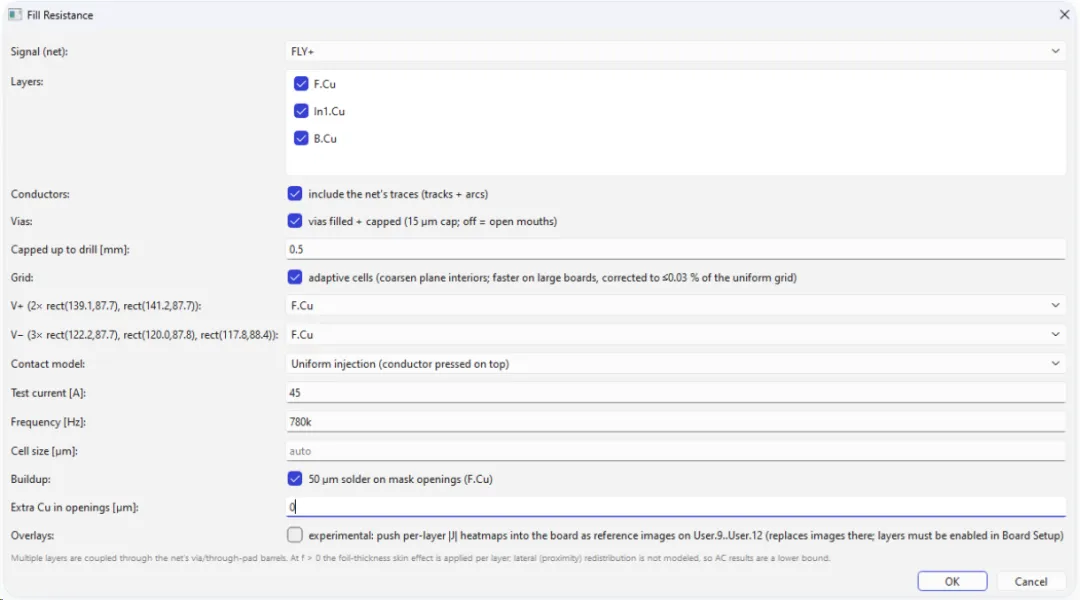 Classic mode parameter settings: net, copper layers, test current, frequency, grid, via model and optional overlay options are configurable.
 -
Inspect resistance, voltage drop, power and current crowding
After solving, the plugin produces per-layer PNG maps, a textual summary and geometric data. You can clearly see where voltage drops concentrate, which copper region is the bottleneck, which vias carry more current, and the total loss at the tested current.
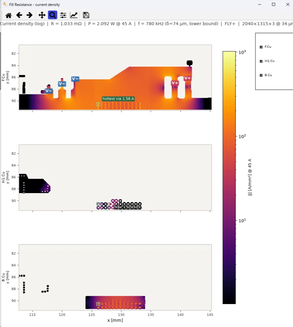 Real power board example: the summary header shows total resistance and loss; the image also marks the busiest via.
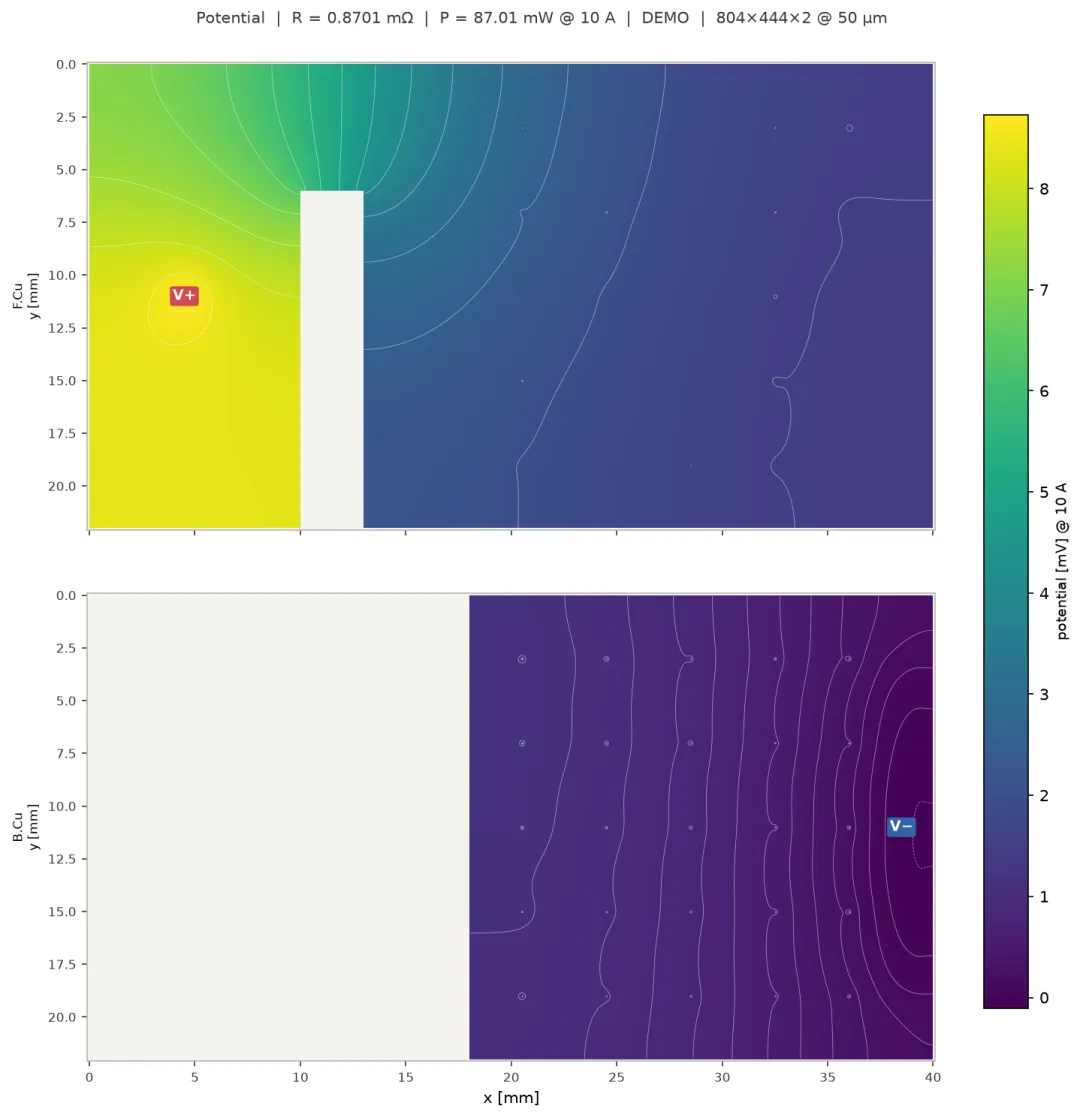 Potential map for the same structure. Denser equipotential lines indicate larger local voltage gradients, quickly locating the main voltage-drop regions.
The real value is not the pretty heatmap, but converting geometric issues into actionable design decisions: should a neck be widened? Should the injection point move? Are there enough vias? Are multiple copper layers actually sharing the current?
PDN mode: upgrade from two-terminal copper resistance to multi-source, multi-load analysis
Since v1.4.0 the plugin includes a PDN mode. Instead of reducing a net to a single V+ and V? group, you can configure any number of power sources and loads on the same power network:
- Each power source can be assigned an output resistance and an open-circuit voltage, acting as a simplified Thevenin source.
- Each load can be given its own current requirement or configured as a voltage probe.
- Results include the actual current provided by each source, the average/minimum voltage at each load contact area, copper IR drop, power loss and per-via currents.
- The plugin also generates a power–load pairing table, reporting effective copper resistance and apportioned loss between pairs of contact points.
Terminals can be defined with rectangles on User.1/User.2 layers and edited directly in the dialog, or saved to and loaded from a JSON configuration for repeated runs under different conditions. From v1.4.2 you can also open the dialog first and then load a saved configuration via "Load config..." even if no objects are preselected on the PCB.
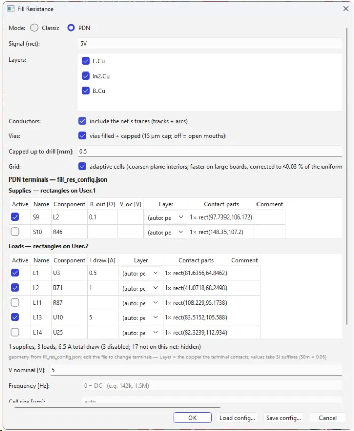
PDN mode: configure supply and load terminals individually, enable/disable terminals and enter output resistance, open-circuit voltage, load current and notes.
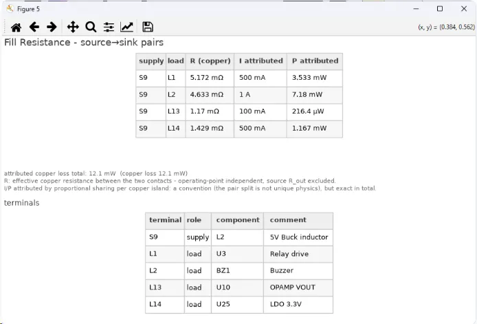
PDN result table: effective copper resistance, allocated current and apportioned power per source–load pair, with terminal names and notes.
How is it computed?
Fill Resistance does not naively convert a copper pour into "length ÷ cross-sectional area." It models each included copper layer as a thin resistive sheet, discretizes the geometry onto a mesh and solves the potential using a multilayer finite-difference method. Via and plated-through-hole walls connect different layers. From the solved potential field the plugin computes current density, power density and the current through each connecting via.
To balance large pours with solver speed, the plugin uses an adaptive grid by default: it refines cells near copper boundaries, pads, vias and narrow regions, and uses coarser elements across large planes. Engineers do not need to understand every solver detail, but should know this is a multilayer resistive-field solver, not a full 3D electromagnetic simulator.
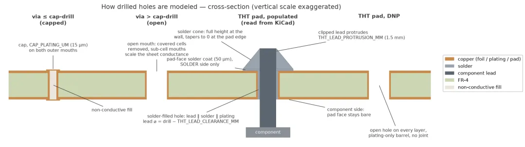
The plugin includes simplified modeling for plugged/unplugged vias, soldered THT pads and unpopulated through-holes. Copper on the via wall, solder and component pins affect inter-layer conduction.
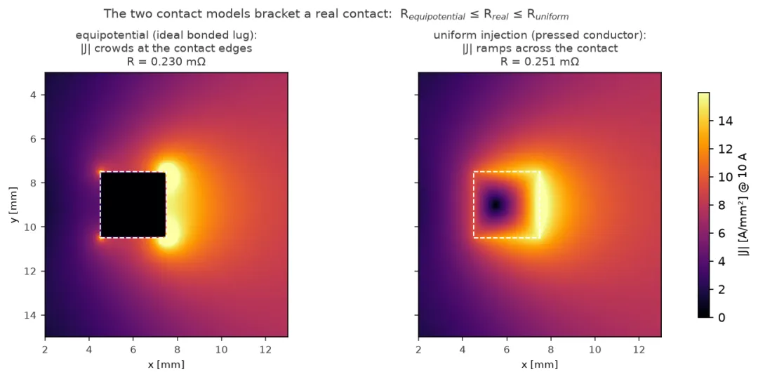
Contact-model comparison: an ideal equipotential terminal and a uniform current-injection terminal produce slightly different current crowding and total resistance.
Installation
- Use KiCad 10.0.1 or later.
- In KiCad, enable the KiCad API from Preferences → Plugins and verify the Python interpreter path is correct.
- Download the plugin PCM package from the project Releases page: th.co.b4l.fill-resistance_1.4.2.zip.
- Open the Plugin and Content Manager in KiCad, click Install from file..., choose the downloaded ZIP and follow the prompts to install.
- Restart KiCad. On first load the plugin will create an isolated Python environment and install dependencies such as NumPy, SciPy, Matplotlib and PySide6. This may take several minutes. After installation an Ω button appears in the PCB editor toolbar.
If the toolbar button does not appear, find the plugin under Preferences → PCB Editor → Action Plugins, right-click and choose Recreate Plugin Environment. Also confirm the API is enabled and the Python path does not point to an older KiCad installation.
Boundaries you must know
| What the plugin is good at | What the plugin cannot do |
|---|---|
| DC copper resistance, static IR Drop, power loss and current distribution | Not a full AC impedance, SI or 3D electromagnetic field solver |
| Multilayer copper pours, traces, pads, vias and plated-through-hole walls | Does not compute inductance, proximity effects, radiation or real EMI return paths |
| Steady-state loss analysis for a specified current | Does not include thermal feedback, transient loading or power-control-loop dynamics |
| Helps compare layout options and locate bottlenecks | Cannot replace final prototype measurements, thermal analysis or high-end PI sign-off |
Note: when frequency > 0 the plugin only applies a correction for skin-effect-induced resistance increase of the copper foil and via walls; it does not include inductance or lateral proximity effects, so the result is not a full AC impedance.
The developers report that a small number of board-level micro-ohm meter measurements were compared to the plugin results, with measured values generally within roughly ±20% of the computed results. That indicates engineering reference value, but it is not a general accuracy guarantee across all board materials, copper thicknesses, plating, soldering and contact methods. Copper-thickness tolerances, via copper thickness, material resistivity, probe placement and contact model selection all influence results.
Designs most worth trying this on
- Low-voltage, high-current PCBs such as battery systems, BMS, inverters, motor drivers, LEDs and power modules
- Irregular high-current paths around MOSFET parallel arrays, connectors, fuses and shunt resistors
- Power networks relying on multilayer copper pours and via arrays to share current
- Scenarios that require comparing "widen copper, add vias, move feed points, adjust load placement" to determine the most effective mitigation
- Teams that want a lightweight static PDN check before fabrication but do not have commercial PI tools
An interesting detail: this is an AI-assisted EDA plugin
The author discloses in forums and the README that a large portion of the plugin code, solver, tests and documentation was produced with assistance from Claude / Claude Code under human guidance and review. The project also uses analytical solutions, convergence tests, power-conservation checks and board measurements to constrain and validate results.
This provides a noteworthy example: AI's value in EDA can extend beyond "auto-routing" to rapidly building specialized engineering tools. The author also cautions users to read model boundaries critically, treat outlier numbers with engineering skepticism, and cross-validate with hand calculations or measurements.






