PCIe 7.0 at 128 GT/s is not simply "make the PCIe 5.0 traces shorter." The real change is this: the link still uses PAM4, with each symbol carrying two bits, but the receiver must recover distortion caused collectively by package, vias, PCB, connectors, crosstalk, jitter, and noise, all under a higher Nyquist frequency and smaller vertical decision margins. If PCB engineers continue to focus solely on "85 Ω differential" and "length mismatch under some mils," it's easy to end up with a board that passes rules yet delivers a channel with little or no margin.
Question: At 128 GT/s, what should be pulled forward in PCB design so that teams move from "layout completed" to "channel sign-off completed"?
PAM4 Turns "Local Correctness" into a Dangerous Illusion
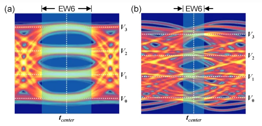
NRZ has two levels; PAM4 has four levels and three decision thresholds. Even with the same peak-to-peak amplitude, the vertical decision intervals are smaller. The result: the same 1 mV noise, the same small via reflection, the same small amount of crosstalk consumes a larger fraction of the available margin in PAM4. PCI-SIG has specified that PCIe 7.0 continues to use PAM4 at a raw data rate of 128 GT/s, which means insertion loss, return loss, mode conversion, and crosstalk at the PCB level must enter the budget earlier.
Accordingly, mature design judgment doesn't ask "can this segment run at 128 GT/s?" but rather: how much of the channel loss budget does this segment consume? How much remains for the package, BGA via transitions, and connectors upstream and downstream? Transmitter equalization and receiver CTLE/DFE compensate frequency-dependent loss; they do not fix all reflections and mode conversion. Betting the entire outcome on equalization is essentially using silicon capability to compensate for PCB uncertainty.
At 128 GT/s with PAM4, the symbol rate is 64 GBd. The first observation point typically falls near the Nyquist frequency around 32 GHz, but that doesn't mean components above 32 GHz can be ignored. Vias, connectors, and edge-related discontinuities can inject higher-frequency content into reflections and mode conversion. Therefore, material models, S-parameter bandwidth, and de-embedding must cover a sufficiently wide frequency range. The goal isn't to memorize a single cutoff number; it's to ensure the model bandwidth covers the physical phenomena you need to explain.
The Most Underestimated Aspect of Vias Isn't Inductance—It's the Return Path
When a high-speed differential pair changes layers, the signal current travels down through the signal via and the return current must transfer from the original reference plane to the new one. If both reference planes are GND and nearby stitching vias are close enough, the return path transitions over a short distance. If the reference switches from GND to power, or there is no suitable reference via nearby, the return current detours. Detours mean a larger high-frequency loop, stronger common-mode conversion, and more energy that should stay in differential mode being converted into radiation and crosstalk.
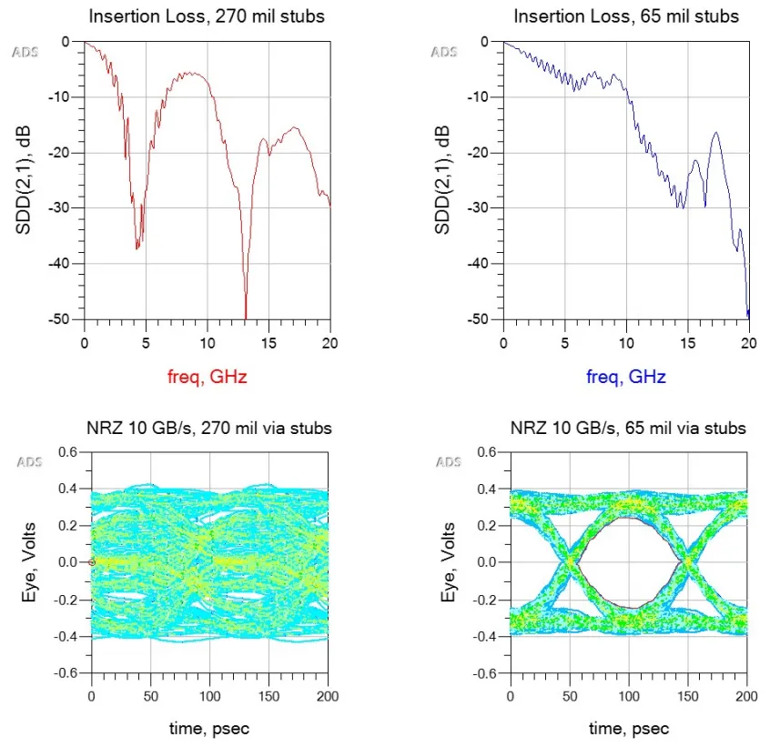
Figure 1 | Impact of via stub length on insertion loss and eye diagram
Therefore, "reduce the number of vias" is an overly crude rule. What truly needs optimization includes: stub length; anti-pad diameter; coupling between the vias in the pair; reference-plane continuity; whether the return path completes locally; and whether via resonances fall within the operating band. At this generation of data rates, critical vias should be modeled in 3D EM rather than relying solely on a single number from a 2D impedance tool.
Also note that "correct differential impedance" does not equate to low mode conversion. Any asymmetry between the two vias—anti-pad size, return via placement, reference-plane openings, or breakout routing—can convert differential mode into common mode. Even if Sdd21 looks acceptable, Scd21/Sdc21 may already expose structural asymmetry. Such issues often worsen EMI at the same time.
Do a Loss Budget Before Layout; Only Then Is Sign-off Meaningful After Layout
Many projects do this backward: finish the board, then export S-parameters to "see the result." The problem is that when simulation reveals excessive loss, BGA fanout, connector locations, stackup materials, and layer counts are already frozen, leaving only local patches. A more efficient approach is to break down the budget during placement and stackup definition: estimate how much the package escape consumes, how much the main traces consume, how much the via pairs consume, how much the connector consumes, and how much margin must be reserved for manufacturing drift and temperature.
| Element | Questions to Answer During Design | Priority Actions if It Fails |
|---|---|---|
| Materials/Stackup | Are Dk/Df and copper-roughness models credible over the target frequency band? | Change materials, shorten the channel, adjust dielectric spacing/trace width, and recalibrate the model |
| BGA/Vias | Are via resonances, stubs, anti-pad sizing, and reference transitions acceptable? | Backdrill, use blind/buried vias, optimize anti-pad or layer transitions |
| Traces | Do insertion loss, differential-to-common mode conversion, and crosstalk fit within the budget? | Increase spacing, change layers, reduce parallelism, and re-plan reference planes |
| Connectors | Do the S-parameters cover the target frequency and the installed structure? | Change connectors or include mounting pads/vias in the model |
| System Channel | Is there statistical margin after Tx/Rx equalization? | Return to the loss budget rather than merely "turn up the equalization" |
Sign-off Must Prove the Design Holds Under Boundary Conditions
If the final report says only "85 Ω ±10%," that isn't high-speed channel sign-off. Proper sign-off must at least answer: which stackup and material model revision was used? Were critical via and connector models derived from 3D EM or from measured S-parameters? What temperature and process corners do the channel models correspond to? Are the equalization parameters fixed or adaptive? In which lane, on which board, and under which manufacturing deviation does the worst-case channel appear?
PCIe 7.0 enters the preliminary FYI testing window in 2026. There remains a long engineering path between "able to simulate" and "able to pass compliance and ship at volume." For PCB teams, the most valuable upgrade is not memorizing another ten layout rules, but establishing a closed loop from loss budgeting, stackup and via/connector modeling, to end-to-end channel simulation and manufacturing validation.
Engineering takeaway: Beyond 128 GT/s, the core PCB capability isn't drawing cleaner traces. It's decomposing the channel budget, pulling uncontrollable factors forward, placing every local structure into an end-to-end model, and ultimately proving through sign-off that "the link retains margin at boundary conditions."