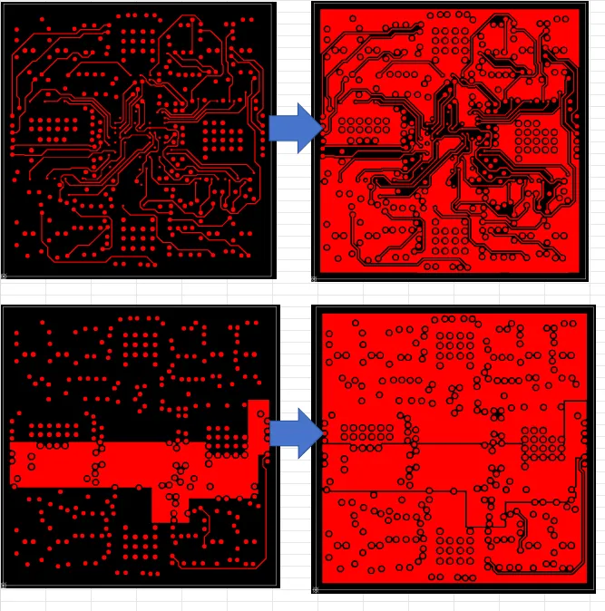
Electromagnetic interference (EMI) issues in high-speed printed circuit boards are often rooted in the same physical mechanisms: fast edges excite wideband energy, discontinuities convert that energy into common-mode currents, and large loops or poorly defined return paths let those currents radiate. The most reliable way to pass emissions and immunity tests is to design EMI out at the schematic and layout stages. The following nine rules distill proven practices that help control EMI without compromising signal integrity (SI) or power integrity (PI).
1. Start with a disciplined stackup and reference-plane strategy
An EMI-resilient design begins with a stackup that provides continuous reference planes and predictable impedance for high-speed traces. Adjacent signal and plane layers minimize loop area and confine fields between the trace and its return path. Poorly chosen stackups force return currents to detour, creating larger loops and higher radiation.
Key considerations include:
- Place each high-speed signal layer adjacent to a solid reference plane (ground is preferable to power for return-path reliability).
- Control impedance by coordinating dielectric thickness, trace width, and copper thickness; consistent impedance reduces mode conversion and reflections.
- Avoid large plane slots and splits under high-speed routes; if splits are functionally necessary, route sensitive signals over continuous ground and bridge splits with stitching capacitors only when absolutely required.
- Plan for connector and edge constraints early so return planes remain continuous to board edges where cables attach.
With a sound stackup, many EMI problems never materialize because return currents naturally flow under the signal, confining the electromagnetic field and reducing radiation.
2. Minimize current loop area and ensure return-path continuity
Radiated emissions are proportional to loop area and current. Reducing the physical area enclosed by a signal and its return path is one of the most effective EMI controls. In practice, this means routing sensitive signals over continuous planes and providing the return path close to any layer transitions.
Practical techniques:
- When a trace changes layers, provide a nearby ground via (stitching via) so the return current can transition through the plane stack with minimal detour.
- Do not cross plane splits with high-speed signals. If crossing is unavoidable, use stitching capacitors tied tightly between the planes and place them adjacent to the crossing to provide an AC return path.
- Keep high di/dt loops, such as clock drivers and switch-mode converters, physically compact and directly referenced to ground.
- Avoid long stubs, test loops, or unused via fences that inadvertently increase loop area.
Maintaining return-path continuity also reduces mode conversion from differential to common mode, a frequent root cause of radiated emissions on cables and enclosures.
3. Control edge rates and impedance discontinuities at the source
EMI spectra are shaped by edge rates: faster edges generate more high-frequency energy. Uncontrolled impedance discontinuities convert this energy into reflections and common-mode currents. Controlling both yields significant EMI reduction without sacrificing functional margins.
Recommended practices:
- Where compatible with timing, use series damping resistors at the driver to moderate edge rates and reduce overshoot and ringing. Place the resistor close to the source to maximize damping effectiveness.
- Maintain consistent impedance along the entire path, avoiding abrupt width changes, acute bends, unused stubs, or poorly placed test points.
- Mitigate via stubs by choosing appropriate drilling techniques and by removing unnecessary test pads or long through-hole structures on fast nets.
- Match terminations to the line and topology to minimize reflections; consistent SI often directly translates into lower EMI.
Reducing discontinuities not only improves signal quality and eye openings but also reduces the conversion of differential energy into radiating common-mode components.
4. Route differential pairs as balanced systems and control coupling
Differential signaling is inherently EMI-friendly when implemented correctly. Imbalances, skew, and poor reference continuity convert differential energy to common mode, negating the benefits.
Implement differential pairs with:
- Tight intra-pair coupling and consistent spacing to maintain constant differential impedance.
- Symmetry through bends, vias, and connectors to keep the pair balanced and minimize common-mode generation.
- Short, matched-length routes to control skew; target topologies that minimize stubs and branch discontinuities.
- Reference-plane continuity beneath the pair; if layer changes are required, use paired vias and provide nearby stitching vias to maintain the return path symmetry.
Keep aggressor traces at an appropriate distance to reduce crosstalk. When coupling is unavoidable, orthogonal routing between adjacent layers helps reduce broadside coupling and lowers the chance of common-mode conversion.
5. Treat clocks and periodic aggressors as radiators to be contained
Clocks and repetitive digital patterns concentrate energy at fundamental and harmonic frequencies, making them prime EMI contributors. The design goal is to minimize their loop area, keep them close to ground reference, and prevent them from coupling into cables and enclosures.
Practical steps include:
- Place clock sources centrally or close to the loads they serve to minimize trace lengths and loop area.
- Route clock nets over solid ground planes and avoid plane splits or long layer transitions.
- Provide controlled terminations and, where applicable, consider source damping to reduce ringing.
- Prevent clock lines from running parallel to long I/O or connector routes that can act as antennas.
If the system supports it, techniques such as spreading spectral energy at the source can reduce peak emissions, but they must be balanced with timing and functional requirements.
6. Engineer the PDN for low impedance across frequency
An effective power distribution network (PDN) provides a low-impedance return for switching currents and limits voltage ripple, which in turn reduces EMI. Poor decoupling or high mounting inductance allows current to spread unpredictably across the board and into cables or chassis.
PDN design practices that help EMI:
- Use a hierarchy of decoupling capacitors close to IC power pins, with minimal loop inductance. Optimize via placement and count to reduce mounting inductance.
- Provide solid ground planes and, when possible, pair power planes with ground planes to form parallel-plate capacitance that supports high-frequency current return.
- Avoid excessive reliance on split power planes for isolation; splits can interrupt return paths and increase emissions if not carefully bridged for AC currents.
- When isolation components such as ferrite beads are used, ensure they do not compromise the high-frequency return path needed by nearby signals.
An engineered PDN stabilizes the current paths and reduces both differential- and common-mode noise that would otherwise radiate.
7. Treat connectors, cables, and chassis as part of the RF system
Most compliance failures occur at interfaces. Cables, enclosures, and connectors can efficiently radiate any common-mode energy they receive. Designing the PCB-to-chassis interface thoughtfully is essential.
Recommended interface practices:
- Provide a defined high-frequency reference from PCB ground to chassis at connector entries, using a short, low-impedance path. Techniques include stitching vias, a ground ring around the board edge, and strategically placed capacitive connections where direct bonding is not possible.
- Place I/O filtering components, such as common-mode chokes or RC filters, as close as possible to the connector to confine noise before it reaches the cable.
- Avoid routing high-speed or noisy traces along board edges without a reference guard; consider via fences along edges to confine fields when compatible with the layout and stackup.
- Maintain continuous reference planes up to the connector pins; avoid last-minute neck-downs or voids that create discontinuities and induce common-mode currents.
By defining the return path at the board edge and filtering right at the connector, you greatly reduce the chance that cables become unintended antennas.
8. Partition the layout and isolate noisy functions from sensitive ones
Placement and routing discipline reduces coupling between noisy and sensitive circuits. Good zoning minimizes the coupling paths and makes return currents more predictable.
Guidelines for partitioning include:
- Place high di/dt sources (DC-DC converters, motor drivers, large digital ASICs) away from sensitive analog or RF sections, and minimize the loop areas of their high-current paths.
- Keep sensitive nodes short and shielded by ground where practical, and avoid running them parallel to noisy aggressors or power switch nodes.
- Avoid gratuitous ground splits; instead, use a continuous ground and guide return currents with placement, routing, and local filtering. If a split is required for functional reasons, carefully define the AC return bridges to prevent unintended detours.
- Route orthogonally between adjacent signal layers to reduce broadside coupling, and maintain adequate spacing between unrelated nets to reduce crosstalk.
Thoughtful partitioning lowers the system's overall susceptibility and emission levels by design, reducing the need for late-stage mitigation.
9. Validate with layout checks and early measurements
Even with careful design, verification is crucial. Implement systematic checks and simple measurements early to catch EMI risks before formal compliance testing.
Suggested validation steps:
- Run rule-based checks for return-path discontinuities, plane crossings, and long stubs on fast nets. Confirm that critical signals always reference a continuous ground plane.
- Review each layer transition of high-speed signals for nearby stitching vias and verify impedance continuity across connectors and flex sections.
- Use near-field probes and a spectrum analyzer during bring-up to identify hot spots around clocks, converters, and connectors. Local fixes such as added stitching vias, improved decoupling, or adjusted damping can be evaluated quickly.
- Check cable and enclosure interfaces under realistic operating conditions; small changes in grounding or filter placement at the connector can dramatically alter emissions.
Early feedback closes the loop between design intent and actual behavior, making final compliance more predictable.
Bringing it all together
EMI control in high-speed PCB design is not about a single fix but about coherent execution across stackup planning, return-path control, signal integrity, PDN design, and interface engineering. Each of the nine rules reinforces the same core objectives: reduce loop area, maintain reference continuity, balance and damp high-speed nets, confine high-frequency currents to known paths, and treat interfaces as RF structures. Applied consistently, these practices reduce the likelihood of costly redesigns and improve both emissions and immunity performance without compromising function or manufacturability.