The stackup is fixed: a four-layer board. Do you keep the third layer as a power plane and go with Signal–Ground–Power–Signal, or do you switch to Signal–Ground–Ground–Signal? Copying a reference design that uses a power plane or deleting your power layer just because someone recommends dual ground both skip a critical step: identify what problem that layer actually solves in your design. A dedicated power plane saves power distribution resources, while dual ground improves the availability and continuity of a reference for traces on both outer layers. These are different engineering benefits, not a universal ranking of good versus bad. The meaningful comparison is: which side will your critical nets use, how are your power rails distributed, and after the change, can the power delivery still work with acceptable voltage drop?
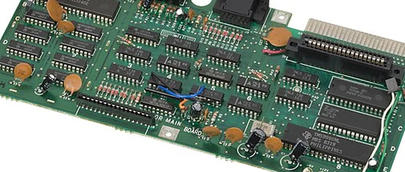
Figure 1 | Chips and interfaces on an assembled board; connectivity needs of functional blocks influence how you allocate layer resources.
Clarify the Job of Layer 3
Let L1 through L4 denote the four copper layers from top to bottom. In a stackup of L1 Signal, L2 Ground, L3 Power, and L4 Signal, the third layer can connect multiple loads with relatively large copper pours. If the primary devices share a common rail and are spread widely, this allocation can reduce congestion from power routing on the outer layers, leaving more space for connectors, device fanouts, and signals.
However, as the number of rails increases, your "power plane" often fragments into multiple islands. Simply labeling a layer as PWR in the stackup is not sufficient. For each copper island, you must define which loads it serves, where the boundaries lie, and whether connections are constricted into necks by pads and vias. The traces, pads, and vias shown in Figure 2 are all finite routing resources; they do not "prove" that any particular stackup is inherently superior.
Therefore, the justification for keeping a dedicated power layer should be: "It solves the power distribution among these devices," not "Four-layer boards are supposed to have a power plane."
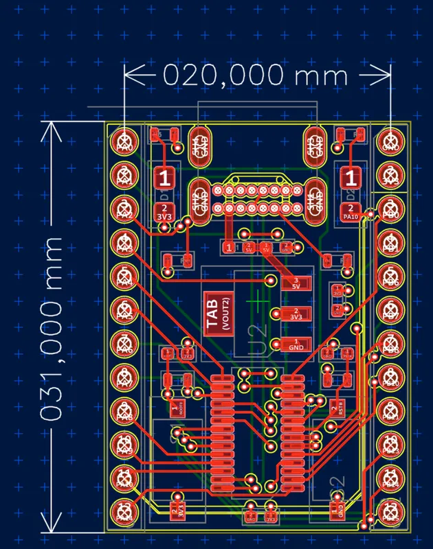
Figure 2 | Pads, traces, and vias share limited space; this image does not establish that one layer order is better than another.
Account for the Reference Plane of Bottom-Layer Signals
In a typical four-layer build where each outer layer is relatively close to its adjacent inner layer, L1 traces primarily couple to L2, and L4 traces primarily couple to L3. The fact that L3 is power copper does not mean L4 cannot carry signals. A continuous power plane can still participate as part of the high-frequency return path. However, the reference relationship between source and receiver, decoupling placement, and any return-path transitions must be intentionally arranged.
Problems arise when the "power layer" is actually divided into several islands, yet the bottom layer is still treated as equivalent to the top in terms of routing conditions. If critical nets primarily use the top layer and the bottom layer carries only a few insensitive connections, keeping the power plane can be perfectly reasonable. If, however, a high-speed interface must rely heavily on the bottom layer, you need to reassess this resource allocation. A shared net name does not substitute for a continuous geometric reference plane.
Do not ignore layer spacing, either. A "four equal horizontal lines" cartoon is just a logical stack, not a physical cross-section. To evaluate coupling strength, calculate trace width, and plan references, use the PCB manufacturer's actual dielectric thicknesses; do not copy a trace width measured from someone else's figure.
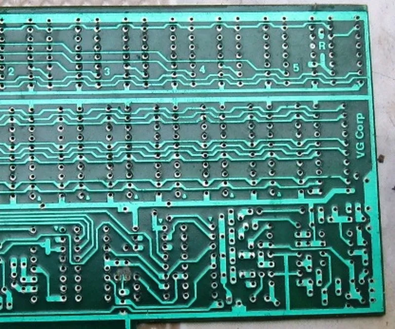
Figure 3 | Traces and solder features on the backside; surface appearance cannot show the completeness of internal reference planes.
Switching to Dual Grounds Doesn't Make Power Go Away
If you change to L1 Signal, L2 Ground, L3 Ground, and L4 Signal, each outer layer more easily gains a continuous ground reference. This is valuable when both outer layers must carry critical connections. However, the power distribution previously handled on the third layer must move to copper pours or routed traces on the outer layers. Since the outer layers also host components, pads, and clearance, you must confirm that they can accommodate this copper by trial routing.
Consider a board with an MCU, a communication interface, and three power rails. If each rail is only consumed within a local region, the power "corridors" on the outer layers are short, and a dual-ground scheme can be straightforward to implement. If one rail must traverse the entire board to supply multiple load groups, and the remaining corridors become narrow after you route around dense components, deleting the power plane may introduce unacceptable voltage drop and self-heating. This is a needs-based comparison, not a measurement conclusion derived from a photo.
When comparing options, focus on the narrowest and most tortuous segments of the power path, not just the total copper area. In Figure 4, you can see copper pours, vias, and isolation gaps coexisting; a large copper fill does not imply a consistently wide path from source to load. Dual ground planes must also be properly interconnected; they should not exist as two independent "green backgrounds."
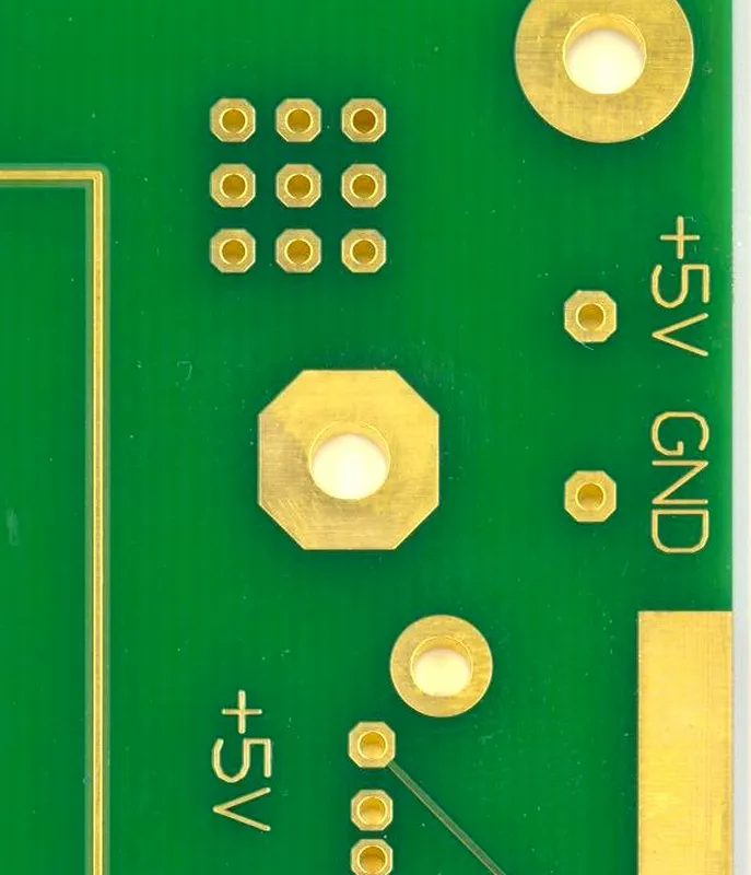
Figure 4 | Local copper pours, connecting vias, and clearance gaps; examine bottlenecks along the power delivery path.
Decide via a Small Routing Trial, Not by Consensus
Start by selecting one of the most challenging signal connections—such as an interface to the main SoC—and one of the most constrained power rails. For both stackup options, perform a placement and short trial route. Record which layer each critical signal uses, the adjacent reference, where layer transitions occur, the minimum corridor for the selected power rail, and the expected current. If these two critical paths cannot be completed, a clean result elsewhere does not make the stackup viable.
Next, verify with your PCB manufacturer the materials, dielectric thicknesses, copper weights, and achievable trace widths to recompute impedance based on the actual cross-section. Estimate DC voltage drops along the power path and include decoupling placement in your review. The cross-sections in Figure 5 simply illustrate how the two schemes allocate resources; they are not to scale and do not imply that either structure will inherently pass EMC.
If both four-layer schemes force you to sacrifice critical connections, revisit the component placement, the overall layout, or your layer count budget. The earlier this decision is made, the easier it is to control rework costs.
Whether layer 3 on a four-layer board is worth dedicating to power depends on whether the power-distribution resources it saves outweigh the reference-plane benefits of a dual-ground scheme. As a next step, run a small trial route for your own critical interface and primary power rail. Map the bottlenecks in both options before finalizing the stack order. Will your design first be constrained by bottom-layer reference conditions for signals, or by insufficient power corridors on the outer layers?