Introduction
Power distribution in printed circuit boards demands reliable methods to handle high currents while maintaining stable voltages across components. Copper pour in power planes serves as a fundamental approach, creating extensive conductive areas that minimize resistance and inductance. Engineers designing for electric applications, such as power supplies and motor drives, rely on these structures to prevent overheating and voltage fluctuations. PCB copper pour power planes distribute power evenly, reducing the risk of hotspots and ensuring consistent performance under load. This article examines the principles, best practices, and considerations for optimizing copper pour current capacity and power plane voltage stability. By understanding these elements, designers can enhance overall board reliability and efficiency.
What Is a PCB Copper Pour Power Plane and Why It Matters
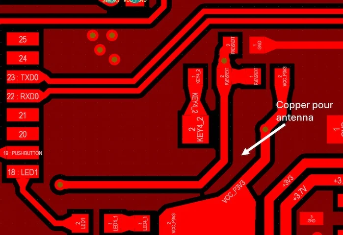
A PCB copper pour power plane consists of a continuous or near-continuous layer of copper etched or filled across an entire PCB layer dedicated to power distribution. Unlike narrow traces, this copper pour current capacity leverages the large cross-sectional area to support substantial currents with minimal voltage drop. Power distribution copper pour also acts as a low-impedance return path, shielding sensitive signals from electromagnetic interference. In high-density boards, these planes occupy inner layers, sandwiched between signal layers for optimal routing.
The relevance stems from the growing demands of modern electronics, where components draw peak currents that challenge traditional trace-based distribution. Inadequate power planes lead to excessive IR drops, causing logic errors, reduced margins, and premature failures. Effective power plane voltage stability ensures uniform supply to ICs, critical for analog and digital circuits alike. Standards like IPC-2221 outline generic requirements for such designs, emphasizing uniform copper distribution to avoid voids that compromise integrity. Ultimately, well-designed copper pours enable compact layouts without sacrificing thermal or electrical performance.
Technical Principles of Copper Pour in Power Planes
Copper pour functions through basic electrical properties, where resistance follows the formula R = ρL/A, with ρ as copper resistivity, L as length, and A as cross-sectional area. In power planes, the vast width maximizes A, drastically lowering R compared to traces, thus boosting copper pour current capacity. Thickness, typically 1 to 3 ounces per square foot, further enhances this by increasing A vertically. Heat dissipation plays a key role, as current generates I2R losses that raise temperature, potentially delaminating the board if unchecked.
IPC-2152 provides charts correlating current, width, thickness, and allowable temperature rise for conductors, applicable to plane segments. For full planes, capacity exceeds trace limits due to spreading currents, but edge effects and splits require analysis. Voltage stability arises from low plane impedance, combining resistance and inductance. Inductance L scales inversely with area, so broad pours minimize di/dt-induced drops during transients. Power plane voltage stability also benefits from capacitance to adjacent ground planes, forming a distributed LC filter that suppresses noise.
Dynamic loads amplify these effects, where switching currents cause ripple. Uniform copper pour ensures even potential across the plane, preventing ground bounce. Voids or islands in the pour increase local resistance, leading to instability. Multilayer designs use via stitching to connect split pours, maintaining continuity. These principles guide engineers in balancing current handling with signal integrity.
Factors Influencing Current Capacity and Voltage Stability
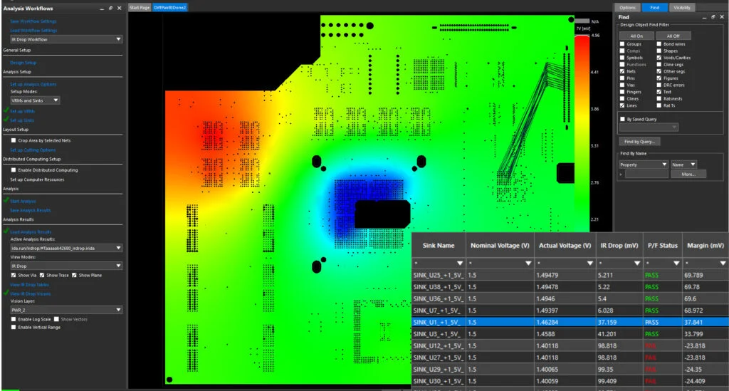
Current capacity hinges on copper weight, board thickness, and ambient conditions. Heavier copper reduces resistance but complicates etching and plating uniformity. In power distribution copper pour, thermal vias transfer heat to other layers, extending capacity. However, airflow and component placement affect cooling, necessitating simulation for validation.
Voltage gradients form along current paths, with longer distances exacerbating drops. Splitting planes for multiple rails requires careful zoning to avoid coupling. IPC-6012 specifies performance criteria for rigid boards, including copper integrity under thermal stress. Decoupling capacitors near loads stabilize voltage by supplying transient currents locally. Plane capacitance, C = εA/d, where d is dielectric thickness, further aids filtering.
Best Practices for Maximizing Performance
Start with layer stackup planning, dedicating full layers to power and ground pours adjacent to each other. Use the thickest feasible copper for high-current sections, tapering where possible. Ensure pours connect to power entry points via wide spokes or multiple vias to equalize distribution. Maintain clearances per IPC-2221 to prevent shorts, especially near splits.
Fill polygons without isolated islands, using thermals for SMD pads to allow solder flow while preserving conductivity. Stitch plane edges with vias every few millimeters to reduce inductance in multilayer boards. Simulate current density and voltage using field solvers to identify weak spots early. For power plane voltage stability, place high-frequency decoupling closest to pins, progressing to bulk caps.
Verify pour completeness post-etching through inspection, as undercuts reduce effective area. In high-reliability designs, anneal copper for better ductility under thermal cycling. These steps align copper pour current capacity with application needs without overdesign.
Common Challenges and Troubleshooting Insights
Hotspots often arise from uneven current spreading, especially near connectors. Analyze paths from sources to sinks, widening bottlenecks. Voltage instability manifests as jitter in clocks; check plane splits overlapping high-speed returns. Use scopes to measure ripple under load.
Voids from poor plating manifest as high-resistance zones, detectable via flying probe tests. Reflow issues warp thin boards with heavy copper, so reinforce with cores. Troubleshooting involves thermal imaging for hotspots and network analyzers for impedance. Case in point, a power converter board saw 10% voltage sag until pours extended fully and vias added.
Conclusion
Copper pour in power planes stands as a cornerstone for robust power distribution, directly impacting current capacity and voltage stability. By applying principles from resistance minimization to impedance control, engineers achieve reliable designs. Best practices like stitching and simulation ensure manufacturability. Adhering to standards fortifies these efforts, yielding boards that perform under demanding conditions. Prioritizing PCB copper pour power plane optimization leads to enhanced system margins and longevity.
FAQs
Q1: What factors primarily determine copper pour current capacity in power planes?
A1: Copper thickness, pour area, and temperature rise limits dictate copper pour current capacity, as outlined in IPC-2152. Larger areas spread current evenly, reducing density and heat. Ambient cooling and via connections further boost handling. Designers must balance these with etching feasibility for optimal results.
Q2: How does power distribution copper pour improve power plane voltage stability?
A2: Power distribution copper pour lowers resistance and inductance, minimizing IR drops and transient spikes for better power plane voltage stability. Adjacent ground planes add capacitance, filtering noise. Uniform fills prevent local gradients. Strategic decoupling enhances this effect across loads.
Q3: Why avoid voids in PCB copper pour power planes?
A3: Voids raise local resistance, compromising copper pour current capacity and causing voltage instability in PCB copper pour power planes. They concentrate current, leading to hotspots. Proper polygon rules and inspections eliminate them. This maintains uniform distribution per design standards.
Q4: What role do vias play in multilayer power plane designs?
A4: Vias stitch pours across layers, equalizing potentials and enhancing power plane voltage stability. They reduce inductance in splits, supporting high currents. Place arrays along edges and zones. This practice aligns with IPC-2221 guidelines for reliable power distribution.
References
IPC-2152 — Standard for Determining Current-Carrying Capacity in Printed Board Design. IPC, 2009
IPC-2221B — Generic Standard on Printed Board Design. IPC, 2012
IPC-6012E — Qualification and Performance Specification for Rigid Printed Boards. IPC, 2018


