Introduction
Copper pours form essential elements in modern PCB design, serving as ground planes, power distribution networks, and thermal management features. Among PCB copper pour types, hatched and solid variants stand out for their distinct impacts on electrical, thermal, and mechanical performance. Electric engineers often face the challenge of selecting the optimal approach based on specific application needs, such as high-speed signal integrity or power handling. This decision influences copper pour EMI performance, copper pour heat dissipation, and overall board reliability. Understanding the trade-offs between hatched copper pour and solid copper pour enables designers to balance functionality with manufacturability. This article provides a structured comparison to guide informed choices in PCB layouts.
Understanding Copper Pour in PCB Design
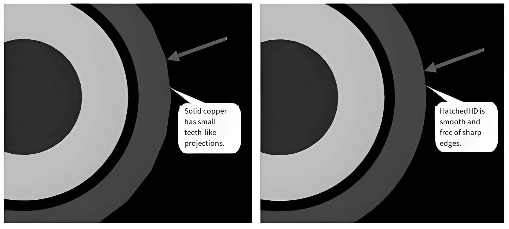
Copper pour refers to filling unused areas on PCB layers with copper connected to a specific net, typically ground or power. This practice minimizes impedance variations and provides a low-inductance return path for signals. Solid copper pour creates a continuous sheet of copper across the designated area, offering uniform coverage. In contrast, hatched copper pour employs a grid or crosshatch pattern, where copper lines intersect with open spaces, usually occupying 20 to 50 percent of the area. These PCB copper pour types emerged to address evolving demands in multilayer boards, from high-frequency circuits to flexible designs.
Designers implement pours during the layout phase to enhance overall board performance without altering trace routing.
Electrical Performance: Impact on EMI and Signal Integrity
Solid copper pour excels in copper pour EMI performance due to its continuous structure, which forms an effective shield against electromagnetic interference. The unbroken plane provides a stable reference for return currents, reducing loop inductance and radiated emissions in high-speed designs. Hatched copper pour, however, introduces gaps that can increase effective inductance, potentially degrading EMI shielding and allowing more crosstalk between traces. Engineers must consider operating frequencies; above 1 GHz, solid pours maintain better impedance control per layer stackup analysis. While hatched patterns suffice for low-frequency applications, they demand careful stitching vias to mitigate field penetration. Overall, solid pours align with requirements for stringent EMI compliance in dense, multilayer boards.
Thermal Management: Heat Dissipation Characteristics
Copper pour heat dissipation relies heavily on the copper volume and connectivity within the pour area. Solid copper pour offers superior thermal spreading, acting as an extended heat sink for adjacent components like power ICs or resistors. Its high thermal conductivity efficiently conducts heat away from hotspots, lowering peak temperatures during operation. Hatched copper pour, with reduced copper density, exhibits limited heat dissipation capacity, as gaps interrupt thermal paths and concentrate heat in narrower lines. This difference becomes critical in power electronics, where solid pours prevent thermal runaway more effectively. Designers evaluate junction-to-ambient thermal resistance when selecting pour types for heat-intensive layouts.
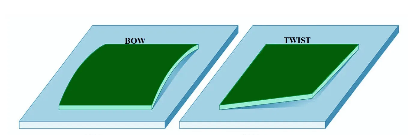
Mechanical and Manufacturing Considerations
Uneven copper distribution across layers can induce warpage due to coefficient of thermal expansion mismatches between copper and the substrate. Solid copper pour amplifies this risk on outer layers, as large expanses contract differently during lamination or reflow cycles. Hatched copper pour mitigates stress by allowing substrate expansion through voids, promoting dimensional stability in asymmetric stackups. IPC-2221 guidelines emphasize balanced copper density to control warpage within acceptable limits for rigid boards. In flex or rigid-flex designs, hatched patterns enhance bend radius tolerance by reducing stiffness. Manufacturing benefits from hatched pours include shorter etch times and improved solder mask adhesion over patterned surfaces.
Comparing PCB Copper Pour Types: Key Metrics
This section highlights trade-offs, aiding quick assessment for project constraints. Solid pours suit performance-critical rigid boards, while hatched variants prioritize mechanical reliability.
- EMI Performance: Solid - excellent shielding, low inductance; Hatched - moderate, gaps increase interference.
- Heat Dissipation: Solid - high thermal conductivity, even spreading; Hatched - reduced capacity, potential hotspots.
- Warpage Risk: Solid - higher if unbalanced; Hatched - lower due to stress relief.
- Flexibility Suitability: Solid - limited, stiffens board; Hatched - better for dynamic bending.
- Manufacturing Cost: Solid - higher etching volume; Hatched - lower material use.
Best Practices for Implementing Copper Pours
Start with copper balancing across all layers to comply with IPC-6012 qualification criteria for flatness. Use solid copper pours on inner power and ground planes for optimal EMI and thermal benefits in high-density designs. Reserve hatched copper pours for outer layers or flex regions to minimize warpage during thermal cycling. Incorporate via stitching around pour boundaries at intervals no greater than one-tenth of the wavelength to maintain continuity. Simulate EMI and thermal profiles early to validate choices against application requirements. Adjust hatch spacing, typically 0.1 to 0.5 mm lines with equal voids, based on board thickness and frequency needs.
In multilayer stackups, combine types strategically: solid inner for performance, hatched outer for balance. Test prototypes for warpage post-lamination, targeting levels below industry thresholds. This layered approach maximizes copper pour EMI performance and heat dissipation without compromising yield.
Conclusion
Selecting between hatched copper pour and solid copper pour hinges on prioritizing copper pour EMI performance, copper pour heat dissipation, or mechanical stability in PCB design. Solid pours deliver unmatched electrical and thermal advantages for rigid, high-performance boards, while hatched variants excel in warpage control and flexibility. Adhering to standards like IPC-2221 ensures reliable outcomes across applications. Engineers benefit from evaluating stackup symmetry and simulation data upfront. Ultimately, the right PCB copper pour types enhance signal integrity, power efficiency, and longevity. Thoughtful implementation turns potential trade-offs into design strengths.
FAQs
Q1: What is the main difference between hatched copper pour and solid copper pour?
A1: Hatched copper pour features a grid pattern with voids for stress relief, while solid copper pour forms a continuous sheet. The former reduces warpage risk in multilayer boards, but the latter provides better copper pour EMI performance through lower impedance paths. Heat dissipation favors solid types due to greater copper area. Choose based on flex needs versus electrical demands, ensuring layer balance per design guidelines.
Q2: When should electric engineers use hatched copper pour over solid?
A2: Opt for hatched copper pour in flex PCBs, outer layers prone to warpage, or designs with asymmetric copper distribution. It improves thermal expansion matching and flexibility without significant EMI penalties at low frequencies. Solid pours remain preferable for inner planes requiring optimal copper pour heat dissipation. Always verify via simulations for your stackup.
Q3: How does copper pour EMI performance differ between types?
A3: Solid copper pour offers superior EMI shielding with continuous planes that minimize return path inductance and radiation. Hatched versions introduce gaps, raising inductance and potential interference, especially above 1 GHz. Stitching vias help, but cannot fully match solid performance. Prioritize solid for high-speed signals.
Q4: Which PCB copper pour type provides better heat dissipation?
A4: Solid copper pour excels in copper pour heat dissipation, spreading heat efficiently across large areas for power components. Hatched pours limit this due to reduced copper volume and interrupted paths. Use solid on heat-critical layers, balancing with hatches elsewhere to avoid warpage.
References
IPC-2221B - Generic Standard on Printed Board Design. IPC, 2012
IPC-6012E - Qualification and Performance Specification for Rigid Printed Boards. IPC, 2017
IPC-A-600K - Acceptability of Printed Boards. IPC, 2020


