Introduction
In the complex world of PCB design, courtyard areas represent a fundamental safeguard against common assembly pitfalls. These defined zones around component footprints establish minimum clearances for electrical isolation and mechanical handling during manufacturing processes. Proper implementation of PCB courtyard areas ensures reliable component spacing, which is essential for high-yield surface-mount technology assembly. Engineers often overlook these areas in dense layouts, leading to issues like solder bridges or placement inaccuracies that compromise PCB manufacturability. By adhering to established guidelines, designers can mitigate risks and streamline production. This article delves into the principles, best practices, and engineering rationale behind courtyard areas to empower electric engineers in creating robust designs.
What Is a PCB Courtyard Area and Why Does It Matter?
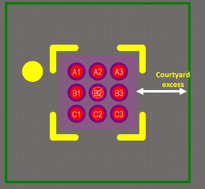
A PCB courtyard area is the rectangular boundary that encompasses a component footprint, including its land pattern, solder joints, and surrounding keep-out space. According to IPC-7351, this zone provides the minimum electrical and mechanical clearance needed to prevent interference between adjacent components during placement, soldering, and inspection. The courtyard excess, measured from the outermost edge of the footprint, varies based on design density levels to accommodate manufacturing tolerances. In high-density boards, insufficient courtyards lead to assembly clearance violations, where pick-and-place machines or reflow ovens cannot operate effectively. Ultimately, these areas directly influence PCB manufacturability by balancing performance with production feasibility. Neglecting them increases defect rates, rework costs, and time-to-market delays for engineering teams.
The relevance of courtyard areas extends beyond initial layout to the entire assembly workflow. In wave or reflow soldering, inadequate component spacing risks bridging or tombstoning, making it one of the most critical high-performance PCB assembly key design considerations for modern manufacturing. For electric engineers, understanding courtyards optimizes signal integrity while ensuring compliance with fabrication capabilities and proactive risk management.

Technical Principles Behind Courtyard Areas
The engineering foundation of PCB courtyard areas lies in their standardization to account for process variations. IPC-7351 outlines three density levels—least, nominal, and most—each with specific courtyard excesses to match fabrication precision. For nominal density, the excess typically ensures 0.25 mm clearance, providing buffer for solder paste deposition and component tilt during reflow. This dimension derives from statistical analysis of placement accuracy, solder volume tolerances, and thermal expansion effects. Electrical principles also factor in, as courtyards maintain creepage distances to prevent arcing under voltage stress. Structurally, the courtyard integrates the component body outline, extended leads, and fiducial considerations for machine vision alignment.
Component spacing rules interconnect with courtyards to form a cohesive layout strategy. Adjacent courtyards must not overlap, creating natural assembly clearance that supports stencil printing and inspection optics. Mechanical stresses, such as board flexure during handling, further justify generous excesses in multilayer stacks. In fine-pitch devices like BGAs, courtyards prevent shadow effects in reflow, where insufficient space causes uneven heating. Engineers calculate these zones by extending footprint perimeters uniformly, verifying against netlist for high-speed signals. This methodical approach aligns design intent with manufacturing physics, reducing variability.
Thermal and mechanical interactions amplify the need for precise courtyards. During reflow, components expand differently, and tight spacing exacerbates warpage-induced shorts. Courtyards accommodate these dynamics, ensuring vias and traces remain uncompromised. For through-hole components, IPC guidelines extend similar principles to hybrid assemblies. Electric engineers benefit from simulating courtyard impacts on airflow and heat dissipation in dense arrays. Overall, these principles transform abstract clearances into tangible safeguards against assembly mishaps.
Best Practices for Implementing Courtyard Areas
Adopt a systematic workflow starting with library footprint verification to embed correct courtyards from the outset. Select density levels based on target manufacturability: nominal for most applications, least for ultra-high density with advanced equipment. Always perform courtyard overlap checks during placement, adjusting positions iteratively for optimal component spacing. Integrate fiducials within or near courtyards to enhance placement accuracy, especially on panels. For double-sided boards, mirror clearances to avoid interference during wave soldering. These steps elevate PCB manufacturability without sacrificing board real estate.
Layer management enhances courtyard efficacy in modern designs. Assign courtyards to a dedicated layer visible in 3D views for rapid violation detection. Combine with silkscreen setbacks to prevent stencil misalignment. In high-reliability applications, exceed nominal excesses by 10-20% for robustness against process drifts. Document courtyard assumptions in fabrication notes, specifying density and tolerance stacks. Electric engineers should collaborate with assembly partners early, validating layouts against their equipment specs. This proactive stance minimizes iterations and boosts yields, particularly when navigating the complex design considerations and challenges of PCB assembly for high-frequency applications. Documenting these assumptions ensures density and tolerance stacks are maintained throughout the production lifecycle.
Toolchain integration streamlines enforcement. Leverage design rule automation to flag encroaching courtyards, coupled with DRC reports for assembly clearance metrics. For mixed-technology boards, harmonize SMT and through-hole courtyards per J-STD-001 criteria. Panelization requires global courtyard padding to accommodate edge effects. Post-layout, generate courtyard overlays for visual review. Best practices culminate in DFM analysis, quantifying risk reductions from proper spacing.
Troubleshooting Common Assembly Mishaps Linked to Courtyards
Assembly defects often trace back to courtyard deficiencies, manifesting as solder shorts or head-in-pillow failures. In one typical scenario, dense QFN arrays with minimal excesses experience bridging due to solder paste squeeze-out under reflow pressure. Engineers diagnose by inspecting X-ray images, revealing overlapped zones where paste volumes exceed clearances. Remediation involves redistributing components, expanding courtyards to nominal levels, and recalculating paste apertures. This logical troubleshooting restores manufacturability while preserving functionality.
Misplacement errors, another courtyard-related issue, arise from nozzle collisions in tight arrays. Symptoms include tilted components and open joints, confirmed via AOI scans. Root cause analysis points to insufficient assembly clearance, violating IPC-2221 spacing minima. Solutions include zoning high-precision areas with larger excesses and adding guard rails in layout. For chronic cases, simulate placement paths to predict interferences. These insights equip engineers to preempt mishaps through courtyard-centric design.
Warpage exacerbates courtyard challenges in large panels. Convex bowing compresses inner courtyards, promoting shorts during pick-and-place. Mitigation strategies employ panel fiducials and symmetric courtyard distributions. Post-assembly yield data validates adjustments, closing the feedback loop. Troubleshooting refines intuition, making courtyard mastery a cornerstone of engineering expertise.
Conclusion
PCB courtyard areas stand as indispensable elements in averting assembly mishaps through disciplined component spacing and clearance management. By embedding IPC-defined excesses, engineers secure electrical integrity and mechanical reliability across the production chain. Best practices like density-matched sizing and rigorous DRCs transform potential pitfalls into strengths, enhancing overall manufacturability. As boards shrink and densities rise, courtyard adherence remains a non-negotiable for electric engineers pursuing flawless execution. Integrating these principles yields designs that assemble predictably, reducing costs and accelerating deployment. Prioritize courtyards to future-proof your PCB innovations.
FAQs
Q1: What is a PCB courtyard area?
A1: A PCB courtyard area defines the minimum keep-out zone around a component footprint, encompassing pads, body, and solder joints for electrical and mechanical clearance. Per IPC-7351, it prevents overlaps that compromise component spacing during assembly. This ensures reliable pick-and-place and reflow processes, directly supporting PCB manufacturability. Engineers use it as a design rule to maintain tolerances.
Q2: How do courtyard areas improve assembly clearance?
A2: Courtyard areas enforce standardized spacing that accommodates placement machine nozzles and solder paste flow. They mitigate risks like bridging or misalignment by providing buffer against process variations. In dense layouts, non-overlapping courtyards guarantee headroom for inspection tools. This practice aligns with assembly standards, boosting yield and reducing rework for electric engineers.
Q3: Why are courtyard excesses critical for PCB manufacturability?
A3: Courtyard excesses, such as nominal 0.25 mm per IPC guidelines, account for tolerances in printing, placement, and reflow. Insufficient excesses lead to shorts or defects in high-volume production. Selecting appropriate density levels optimizes space usage while ensuring feasibility. Engineers verify via DRC to confirm manufacturability from schematic to fab.
Q4: What role do standards play in defining PCB courtyard areas?
A4: Standards like IPC-7351 provide tiered courtyard dimensions tailored to density and process capability. They standardize component spacing for consistent assembly outcomes across facilities. J-STD-001 complements by specifying solder joint criteria influenced by clearances. Adherence minimizes variability, empowering reliable PCB designs.
References
IPC-7351B — Generic Requirements for Surface Mount Design and Land Pattern Standard. IPC, 2010
IPC-2221B — Generic Standard on Printed Board Design. IPC, 2012
J-STD-001G — Requirements for Soldered Electrical and Electronic Assemblies. IPC, 2011


