Introduction
In modern electronics, high-speed signal transmission demands precise control over PCB characteristics to maintain signal integrity and minimize electromagnetic interference, or EMI. PCB EMI impedance control emerges as a critical strategy for engineers designing boards that operate reliably in dense, fast-paced environments. Poor impedance matching leads to signal reflections, which degrade performance and radiate unwanted emissions, complicating compliance with regulatory limits. Reducing EMI in PCB design requires integrating controlled impedance with thoughtful layout choices to preserve waveform quality and reduce noise coupling. This article explores PCB design best practices for EMI, focusing on actionable techniques that enhance signal integrity and EMI reduction. Electrical engineers will find structured guidance here to optimize their designs from stackup planning through routing.
Understanding Impedance Control in PCBs
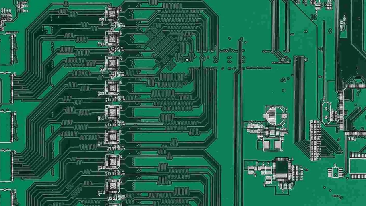
Characteristic impedance in a PCB trace arises from the interaction of inductance, capacitance, resistance, and conductance along the transmission line. For signal integrity, engineers must control this impedance to match source and load characteristics, preventing reflections that distort signals. In multilayer boards, factors like trace width, thickness, dielectric height, and material properties dictate impedance values. Variations in manufacturing tolerances can shift these parameters, underscoring the need for tight process controls during fabrication. Impedance control directly supports signal integrity and EMI by minimizing discontinuities that generate harmonics and radiated noise. Adhering to established guidelines ensures predictable performance across production runs.
EMI Fundamentals and Its Link to Signal Integrity
Electromagnetic interference in PCBs originates from sources such as switching transients, clock edges, and crosstalk between adjacent traces. These emissions couple into nearby circuits or radiate outward, compromising signal integrity through noise injection and bit errors. Signal integrity and EMI are interconnected because reflections from impedance mismatches amplify high-frequency components, increasing susceptibility to and generation of interference. Conducted EMI travels along power lines, while radiated EMI propagates through the air, both challenging high-density designs. Engineers must address these at the layout stage to avoid costly redesigns or shielding add-ons. Understanding these mechanisms allows for proactive impedance and noise reduction strategies.
Principles of Impedance Control for EMI Mitigation
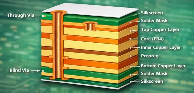
Impedance control begins with stackup design, where alternating signal and plane layers provide return paths and stable reference planes. Microstrip traces on outer layers offer easier impedance calculation but higher radiation risk, while striplines embedded between planes reduce EMI by containing fields. Dielectric materials with consistent epsilon_r values minimize variations, and symmetric builds prevent warpage that alters clearances. Engineers calculate impedances using field solvers during design, specifying tolerances like plus or minus 10 percent for critical nets. This approach aligns with IPC-2141 guidelines for controlled impedance in high-speed boards, ensuring low reflections. Proper control thus serves as a foundation for reducing EMI PCB design challenges.
Stackup Optimization for Signal Integrity and EMI
A well-planned stackup is paramount for PCB EMI impedance control. Place high-speed signals between ground planes to confine fields and lower loop inductance, which curbs radiated emissions. Dedicate inner layers to power and ground, splitting them only when necessary and stitching with vias to maintain low impedance. Core and prepreg thicknesses directly influence dielectric spacing, so select combinations that achieve target impedances without excessive trace widths. Signal integrity improves as crosstalk diminishes in tightly coupled structures. This configuration also aids thermal management, as planes spread heat evenly.
Routing Techniques for Impedance and Noise Reduction
Trace routing profoundly impacts impedance and noise reduction. Maintain consistent widths for controlled impedance traces, avoiding abrupt changes that introduce stubs or mismatches. Route differential pairs with equal lengths and tight spacing to preserve common-mode rejection and minimize skew. Keep high-speed lines away from edges and cuts in planes to avoid fringing fields that boost EMI. Use 45-degree bends over 90-degree corners to reduce reflections, and minimize via count with back-drilling for long traces. These PCB design best practices EMI directly lower susceptibility to external noise while curbing emissions.
Ground stitching vias along signal paths provide low-inductance returns, bridging splits and reducing slot antenna effects. Place them every quarter wavelength of the highest frequency, ensuring solid continuity. Guard traces or moats separate analog and digital sections, blocking crosstalk paths. Ferrite beads or filters on power lines suppress conducted EMI entering the board.
Component Placement and Decoupling Strategies
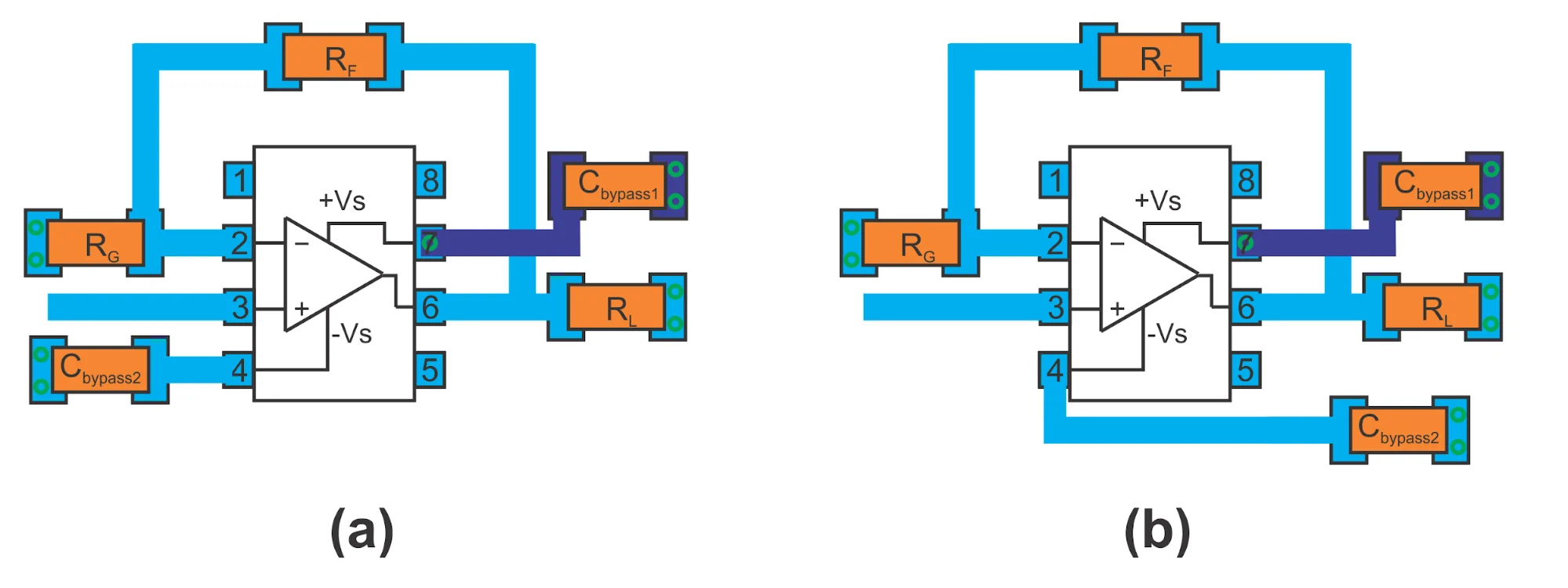
Strategic component placement enhances signal integrity and EMI performance. Position drivers and receivers close together to shorten critical nets, reducing opportunities for noise pickup. Group noisy components like switching regulators away from sensitive analog circuits, with dedicated ground returns. Decoupling capacitors must sit as near as possible to power pins, using arrays for broad frequency coverage. Values selected for local bypass form LC filters that shunt high-frequency noise to ground. Plane capacitance between power and ground layers provides additional bulk decoupling at low frequencies.
Grounding and Shielding Best Practices
Effective grounding forms the backbone of reducing EMI PCB design efforts. Implement a single-point ground for low-frequency analog to avoid loops, transitioning to multi-point for digital at higher speeds. Flood unused areas with ground copper, connecting to planes via dense via fields for image current flow. Via fencing around connectors shields I/O ports, directing return currents and attenuating emissions. Enclosures with conductive gaskets complete the Faraday cage when board-level measures fall short. These techniques, combined with impedance control, yield robust signal integrity.
Following IPC-2221 principles for PCB layout reinforces these practices by specifying clearances and plane integrity. Consistent application prevents common pitfalls like ground bounce.
Verification and Testing for Compliance
Pre-layout simulations predict impedance profiles and EMI hotspots using 3D field solvers. Post-layout extractions feed into time-domain reflectometry models to verify matches. Fabricated boards undergo TDR measurements for impedance profiling and near-field scans for emission mapping. Spectrum analyzers quantify radiated EMI, guiding iterations. These steps confirm that signal integrity and EMI goals align with design intent. Early detection avoids field failures.
Conclusion
Mastering PCB impedance control and EMI reduction demands integrated approaches from stackup to verification. Key practices like plane-proximal routing, stitching vias, and precise decoupling directly bolster signal integrity while curbing emissions. Engineers benefit from standards like IPC-2141 and IPC-2221 to standardize these efforts across projects. Implementing these PCB design best practices EMI ensures reliable performance in high-speed applications. Prioritize simulation and measurement to refine designs iteratively. Ultimately, these strategies minimize risks and optimize board functionality.
FAQs
Q1: What role does PCB EMI impedance control play in high-speed designs?
A1: PCB EMI impedance control prevents signal reflections that degrade waveforms and generate harmonics, key culprits in EMI. By matching trace impedance to driver and receiver specs, engineers reduce overshoot, ringing, and crosstalk. This maintains eye diagrams and bit error rates, essential for signal integrity and EMI compliance. Stackup planning and routing consistency amplify these benefits in dense layouts.
Q2: How can reducing EMI PCB design improve signal integrity and EMI performance?
A2: Reducing EMI PCB design involves solid ground planes, minimal loop areas, and decoupling to shunt noise. These lower radiated and conducted interference, preserving clean signals on high-speed nets. Differential routing and via shielding further isolate paths, cutting crosstalk. Overall, cleaner power delivery and return currents enhance impedance stability and noise immunity.
Q3: Why is impedance and noise reduction critical in multilayer boards?
A3: Impedance and noise reduction in multilayer boards counters field fringing and coupling between layers. Symmetric stackups with embedded signals contain emissions better than surface routes. Stitching and guard traces block unwanted paths, while consistent dielectrics hold tolerances. This setup supports signal integrity and EMI by minimizing discontinuities across frequencies.
Q4: What are essential PCB design best practices EMI for electrical engineers?
A4: PCB design best practices EMI include prioritizing ground returns, controlling trace geometries, and verifying with TDR. Separate noisy and quiet zones, use short paths for clocks, and add fences at edges. Simulations guide layout, ensuring impedance matches and low emissions. These steps deliver compliant, high-integrity boards without excess shielding.
References
IPC-2141A — Controlled Impedance Circuit Boards and High Speed Logic Design. IPC, 2000
IPC-2221B — Generic Standard on Printed Board Design. IPC, 2012
IPC-6012E — Qualification and Performance Specification for Rigid Printed Boards. IPC, 2017


