Introduction
In RF PCB design, the footprint serves as the critical interface between components and the transmission lines that carry high-frequency signals. Proper optimization ensures minimal signal loss, precise impedance matching, and reliable performance in applications ranging from wireless communications to radar systems. Engineers face unique challenges at RF frequencies where even minor deviations in pad geometry or trace width can lead to reflections, attenuation, or crosstalk. This article explores the principles and best practices for designing RF footprints that prioritize low loss PCB characteristics and high efficiency. By focusing on structured engineering approaches, designers can achieve robust signal integrity without compromising manufacturability. Understanding these elements is essential for electric engineers working on next-generation RF systems.
What Is an RF PCB Footprint and Why Does It Matter?
An RF footprint refers to the specific land pattern, including pads, traces, and associated structures, tailored for RF components such as amplifiers, mixers, and antennas on a printed circuit board. Unlike standard footprints, RF versions incorporate transmission line effects to maintain characteristic impedance, typically 50 ohms or 75 ohms, across the entire signal path. This design choice directly impacts insertion loss, return loss, and overall system efficiency. In high-frequency environments, poor footprint design amplifies losses from conductor resistance and dielectric absorption, degrading performance metrics like noise figure and gain flatness. For electric engineers, mastering RF footprint design means balancing electrical performance with fabrication tolerances to meet stringent application demands. As frequencies push into GHz ranges, the relevance of precise RF footprints becomes undeniable for achieving low loss PCB operation.
The matter intensifies in multi-layer boards where footprints must transition seamlessly between surface mounts and embedded striplines. Impedance discontinuities at pad-to-trace junctions can cause voltage standing wave ratios (VSWR) exceeding acceptable limits, leading to power loss and potential component failure. Industry standards like IPC-7351B provide foundational guidelines for land pattern dimensions, ensuring compatibility with surface mount technology while accommodating RF needs. Engineers must consider these footprints early in the RF PCB design process to avoid costly respins. Ultimately, optimized footprints enable minimal loss paths that support higher data rates and longer range in RF systems.
Key Technical Principles in RF Footprint Design
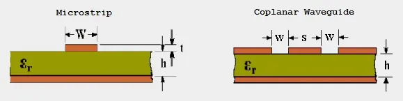
At the core of RF footprint design lies transmission line theory, where the footprint acts as an extension of the controlled impedance structure. Microstrip lines, common on outer layers, require precise trace width and substrate height to achieve target impedance, calculated using formulas that account for dielectric constant and thickness. Conductor losses dominate at lower RF bands due to skin effect, confining current to the surface and increasing effective resistance. Dielectric losses become prominent at higher frequencies, influenced by the material's dissipation factor. For low loss PCB performance, footprints must minimize these effects through rounded corners on pads to reduce field concentrations and reflections.
Impedance matching forms another pillar, ensuring maximum power transfer by matching source, load, and line impedances. Discontinuities arise from pad overhangs or abrupt width changes, modeled using scattering parameters (S-parameters) for prediction. Grounded coplanar waveguide (GCPW) footprints offer superior shielding and lower radiation compared to microstrip, with ground planes flanking the signal trace to stabilize impedance. Via transitions demand careful placement to avoid stubs that resonate at RF frequencies. Adhering to principles in IPC-2141A helps engineers design these transitions with tapered geometries for broadband matching.
Material properties play a pivotal role, as the dielectric constant (Dk) affects line velocity and impedance, while dissipation factor (Df) dictates attenuation. Low loss PCB materials exhibit Df below 0.005 at 10 GHz, essential for minimizing tan delta losses in footprints. Thermal expansion mismatches between components and board can warp footprints during reflow, altering spacing and impedance. Engineers must simulate electromagnetic fields using field solvers to validate footprint integrity before fabrication. These principles ensure that RF footprints support phase stability and amplitude balance across operating bands.
Best Practices for RF Footprint Design
Start with accurate component datasheets to define pad sizes, but adjust for RF using density levels from IPC-7351B, opting for nominal or least density to accommodate wider traces. Maintain symmetry in differential footprints to preserve mode purity and common-mode rejection. For single-ended signals, extend ground vias around pads to form a return path, reducing inductance. Simulate the entire footprint including solder mask effects, as it alters effective dielectric and capacitance. Fabricate prototypes with tight trace width tolerances, typically ±5% or better, to hit impedance targets.
Incorporate stitching vias along transmission line edges to suppress slotline modes and enhance ground return. For low loss PCB designs, route RF footprints on dedicated layers isolated from digital signals to avoid crosstalk. Use embedded resistors or capacitors in footprints for matching networks, ensuring their parasitics align with RF models. During layout, prioritize shorter paths and avoid right-angle bends, favoring 45-degree mitered corners for phase linearity. Compliance with IPC-6018D qualification criteria verifies that fabricated footprints meet high-frequency performance specs like surface finish uniformity and coplanarity.
Layer stackup optimization complements footprint design by providing consistent dielectric heights for repeatable impedance. Blind or buried vias minimize stub lengths in transitions, critical for multi-GHz bands. Post-layout verification involves extracting S-parameters to confirm return loss below -20 dB across the band. These practices collectively minimize insertion loss to under 0.5 dB per inch at 10 GHz. Electric engineers should iterate designs with fabricator input on etch factors and plating variations early.
Common Challenges and Troubleshooting in RF Footprint Optimization
One frequent issue is impedance drift from fabrication tolerances, where trace etch variation shifts Z0 by 5-10 ohms. Troubleshoot by specifying enhanced process controls and measuring test coupons on panels. Solder fillet buildup under components can detune footprints, addressed by precise stencil apertures and reflow profiling. Crosstalk between adjacent RF footprints spikes if ground spacing exceeds lambda/20; mitigate with guard traces or deeper cuts in ground planes.
Via resonance plagues transitions, manifesting as passband ripples; backdrilling or via fences resolve this by shortening stubs. Thermal management challenges arise in power RF footprints, where hotspots elevate Df; integrate heat sinking vias and thermal pads. Simulate worst-case scenarios including material anisotropy for robust designs. Field probing on prototypes reveals hotspots, guiding refinements. These troubleshooting steps ensure low loss PCB reliability in production.
Conclusion
Optimizing RF PCB footprints demands a holistic approach integrating transmission line principles, precise geometries, and material selection for impedance matching and low loss performance. By applying best practices like symmetric layouts, via optimization, and standard-compliant dimensions, engineers can minimize reflections and attenuation. Key to success lies in simulation, fabrication awareness, and verification to deliver high-efficiency RF systems. Electric engineers benefit from these strategies in achieving superior signal integrity across frequencies. Prioritizing RF footprint design elevates overall board performance, paving the way for advanced applications.
FAQs
Q1: What role does impedance matching play in RF footprint design?
A1: Impedance matching in RF footprint design prevents reflections by ensuring continuity between component leads, pads, and traces at 50 ohms typically. Discontinuities cause return loss, increasing insertion loss in low loss PCB setups. Use field solvers to adjust pad shapes and trace widths per IPC-2141A guidelines. Verify with S-parameter tests post-fabrication for optimal performance.
Q2: How can engineers achieve low loss in RF PCB footprints?
A2: Low loss RF PCB footprints rely on materials with low Df, precise etch tolerances, and GCPW structures to reduce radiation. Minimize conductor length and use smooth surface finishes to combat skin effect. Stitching vias enhance shielding. Simulations predict attenuation before build, ensuring under 1 dB loss at operating frequencies.
Q3: Why follow IPC standards in RF PCB design?
A3: IPC standards like IPC-7351B standardize land patterns for reliable RF footprints, promoting interoperability and manufacturability. They guide impedance control and high-frequency qualification per IPC-6018D. Adherence reduces respin risks and ensures performance consistency. Engineers gain confidence in designs meeting industry benchmarks.
Q4: What are common mistakes in RF footprint layouts?
A4: Common errors include neglecting solder mask effects on capacitance and oversized pads causing mismatches. Insufficient ground vias lead to poor return paths, elevating losses. Avoid routing RF near edges without fencing. Always simulate full structures for accurate RF PCB design outcomes.
References
IPC-7351B — Generic Requirements for Surface Mount Design and Land Pattern Standard. IPC, 2010
IPC-6018D — Qualification and Performance Specification for High Frequency (Microwave) Printed Boards. IPC, 2022
IPC-2221C — Generic Standard on Printed Board Design. IPC, 2023
IPC-2141A — Design Guide for High-Speed Controlled Impedance Circuit Boards. IPC, 1996


