Introduction
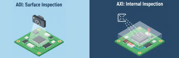
Printed circuit board (PCB) manufacturing demands rigorous quality control to detect defects early and ensure reliability in electronic assemblies. Among various PCB inspection methods, visual inspection and automated X-ray inspection stand out for their roles in identifying issues that could compromise performance. Visual inspection, often enhanced by automated optical inspection (AOI), focuses on surface-level anomalies, while automated X-ray inspection (AXI) penetrates deeper into hidden structures. Engineers must weigh factors like board complexity, defect types, and production volume when selecting the optimal approach for PCB defect detection. This article compares these methods, highlighting their principles, strengths, and applications to guide informed decisions in PCB quality control. By understanding their differences, manufacturers can minimize failures and align with industry benchmarks.
The Fundamentals of Visual Inspection in PCBs
Visual inspection serves as a foundational PCB inspection method, traditionally relying on human operators to scrutinize boards under magnification for surface imperfections. This approach excels at spotting obvious issues such as misaligned components, solder bridges, or insufficient solder volume on accessible pads. However, manual methods introduce variability due to operator fatigue and subjective judgments, prompting the adoption of AOI for consistency. AOI employs high-resolution cameras and sophisticated image processing algorithms to scan boards rapidly, comparing captured images against a golden reference or CAD data. It detects defects like missing parts, polarity errors, and excessive solder fillets with high speed, making it ideal for high-volume surface-mount technology (SMT) lines. Despite its efficiency, visual inspection, including AOI, remains limited to line-of-sight features and struggles with subsurface anomalies.
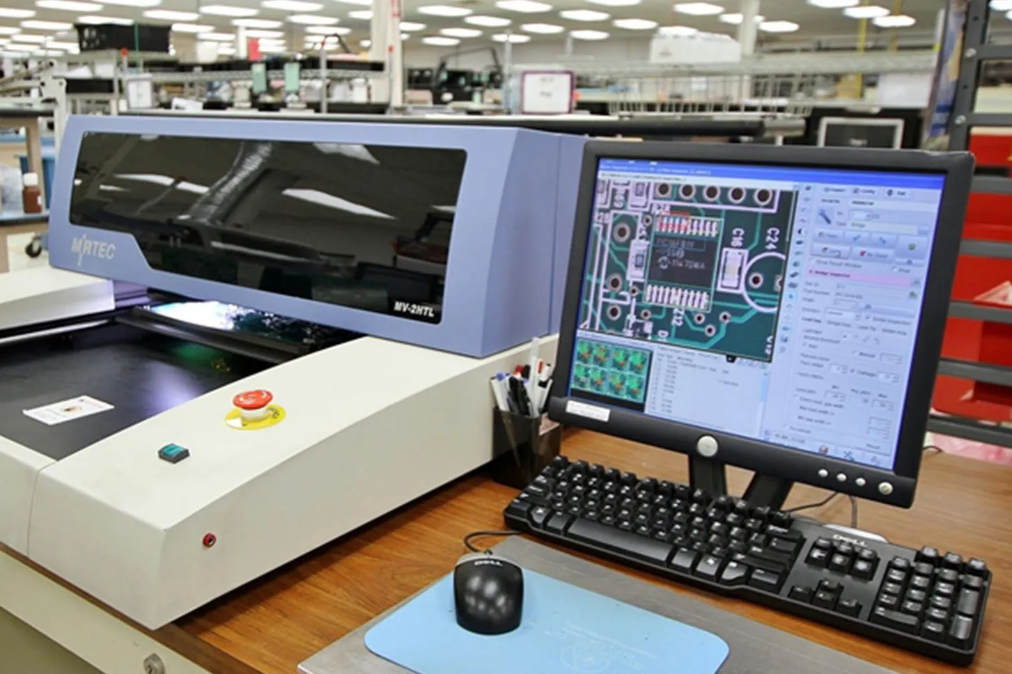
In factory settings, visual inspection aligns with standards like IPC-A-600, which defines acceptability criteria for printed boards, ensuring uniform evaluation across production runs. Engineers appreciate AOI's programmability, allowing customization for specific component libraries and tolerance thresholds. Yet, challenges arise with reflective surfaces or tightly spaced features, where lighting and algorithm tuning become critical. Overall, visual methods provide a cost-effective entry point for PCB quality control, particularly for simpler double-sided boards.
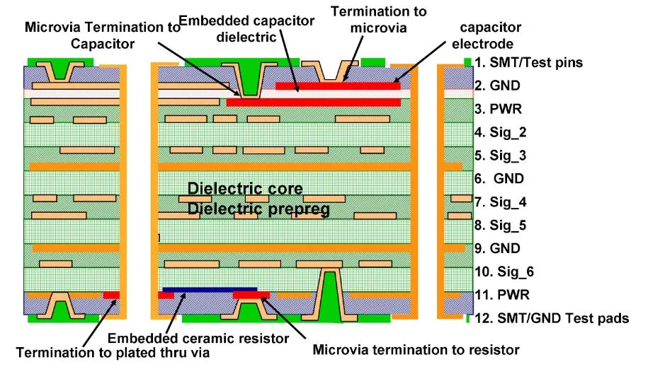
Principles of Automated X-Ray Inspection (AXI)
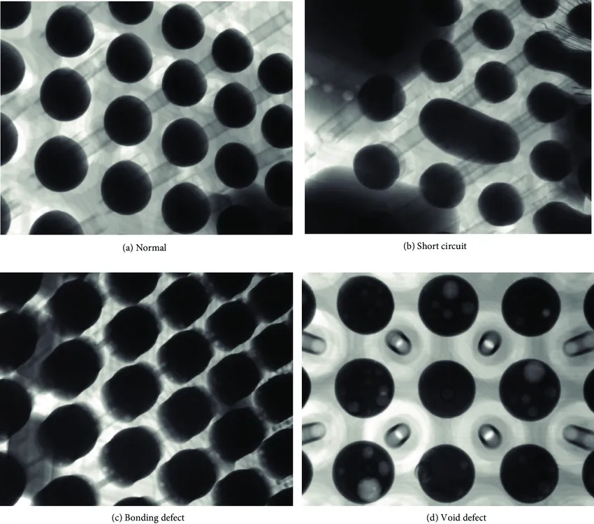
Automated X-ray inspection (AXI) revolutionizes PCB defect detection by using X-ray radiation to generate transmission images of internal structures, bypassing the limitations of optical systems. The process involves directing a focused X-ray beam through the PCB, with detectors capturing varying densities based on material thickness and composition. This reveals hidden features like via fills, barrel cracks, and under-component voids that visual methods cannot access. Modern AXI systems offer 2D and 3D imaging modes, with oblique-angle views enhancing analysis of ball grid array (BGA) solder joints and multi-layer interconnects. Processing software applies grayscale analysis and machine learning to classify defects automatically, reducing human intervention.
AXI proves invaluable for high-density interconnect (HDI) boards and complex assemblies where reliability is paramount. It adheres to guidelines in IPC-6012, which specifies performance requirements for rigid printed boards, including internal integrity checks. While setup requires calibration for beam energy and magnification, AXI delivers precise measurements of joint head-in-pillow effects or tombstoning in inaccessible areas. Factories integrate AXI post-reflow to catch process-induced flaws, complementing other PCB inspection methods.
Technical Comparison: AOI vs. AXI in Defect Detection
Both AOI and AXI form core PCB inspection methods, yet their detection capabilities diverge based on defect location and type. AOI shines in pre-reflow verification, identifying component placement errors, wrong parts, and lifted leads with sub-millimeter precision. In contrast, AXI targets post-reflow issues like solder voids, bridging under chips, and layer misalignment, offering density mapping that optical systems ignore. Speed-wise, AOI processes boards in seconds per side, suiting inline production, whereas AXI demands longer exposure times, often operating offline for intricate panels.
- Primary Focus: AOI - Surface and top-side features; AXI - Internal and hidden structures
- Common Defects: AOI - Misplacement, polarity, bridges; AXI - Voids, cracks, via fills
- Speed: AOI - High (inline capable); AXI - Moderate (often offline)
- Board Suitability: AOI - Low to medium density; AXI - High density, multi-layer
- Cost: AOI - Lower initial investment; AXI - Higher due to equipment
This list illustrates key trade-offs in PCB quality control. AOI's reliance on visible light limits it to external anomalies, while AXI's penetrating rays excel in volumetric analysis. Engineers often combine them for comprehensive coverage, as per J-STD-001 requirements for soldered electrical assemblies.
Best Practices for Selecting PCB Inspection Methods
Choosing between visual inspection and AXI hinges on board design, assembly process, and risk tolerance. For prototypes or low-volume runs with accessible joints, start with AOI to catch assembly errors efficiently. High-reliability applications, such as aerospace or automotive PCBs, necessitate AXI for verifying BGA integrity and via quality, especially in multi-layer stacks. Implement a hybrid strategy: use AOI for 100% inline screening and AXI for sampled high-risk zones to optimize throughput.
Calibrate systems regularly, aligning AOI lighting for uniform illumination and AXI voltages for material-specific contrast. Train operators on IPC-A-600 criteria to interpret outputs consistently, bridging automated and manual reviews. Document inspection thresholds in process control plans, correlating findings with yield data to refine protocols. This factory-driven approach enhances PCB defect detection without excessive downtime.
Troubleshooting Common Challenges in PCB Inspection
In practice, visual inspection falters on shadowed areas under tall components, leading to false calls that slow production. Engineers troubleshoot by adjusting camera angles and reference images, yet persistent gloss issues may require matte sprays. AXI encounters artifacts from dense copper planes, mitigated by multi-angle laminography for clearer 3D reconstructions. A case in point involves HDI boards where AXI revealed 15% void rates in microvias missed by AOI, prompting reflow profile tweaks per IPC-6012 guidelines.
Layer registration errors, detectable only via AXI, often stem from drill misalignment, addressed by enhancing fiducial marks. For cost-sensitive runs, prioritize AOI and reserve AXI for failure analysis, using cross-sectioning to validate X-ray findings. These insights underscore the need for method selection based on defect history and board stackup.
Conclusion
Visual inspection via AOI and automated X-ray inspection represent complementary pillars of PCB quality control, each tailored to specific defect detection needs. AOI delivers rapid, surface-focused scrutiny ideal for high-volume SMT, while AXI provides unparalleled insight into internal flaws for complex assemblies. By evaluating board density, joint types, and production goals, engineers can deploy the right PCB inspection methods to meet reliability standards. Integrating both maximizes yield and minimizes escapes, fostering robust manufacturing processes. Ultimately, strategic selection ensures PCBs perform reliably in demanding applications.
FAQs
Q1: What are the main PCB inspection methods for defect detection, and how do AOI and AXI differ?
A1: Automated optical inspection (AOI) and automated X-ray inspection (AXI) are key PCB inspection methods. AOI uses cameras to check surface features like component alignment and solder appearance, operating at high speeds for inline use. AXI employs X-rays to inspect hidden solder joints and vias, ideal for dense boards. Choose AOI for visible defects and AXI for subsurface issues to optimize quality control.
Q2: When should electric engineers prefer AXI over visual inspection in PCB quality control?
A2: Opt for automated X-ray inspection (AXI) when dealing with BGA packages, multi-layer boards, or vias where defects like voids and cracks hide from view. Visual methods, including AOI, suffice for surface checks but miss internal anomalies. Factory insights recommend AXI sampling post-reflow, aligning with standards for high-reliability assemblies.
Q3: Can AOI fully replace manual visual inspection in PCB defect detection?
A3: AOI enhances manual visual inspection by automating surface defect detection with consistent algorithms, reducing human error in high-volume lines. However, it cannot access undersides or obscured areas, so manual verification remains useful for complex topographies. Combine both for comprehensive PCB quality control, per acceptability criteria.
Q4: What factors influence the choice between AOI and AXI for PCB inspection methods?
A4: Board complexity, defect risk, and throughput dictate selection. AOI suits simple, high-speed production for placement errors, while AXI targets high-density interconnects needing internal analysis. Cost and space constraints also factor in, with hybrids providing balanced PCB quality control.
References
IPC-A-600K - Acceptability of Printed Boards. IPC, 2020
IPC-6012E - Qualification and Performance Specification for Rigid Printed Boards. IPC, 2017
J-STD-001H - Requirements for Soldered Electrical and Electronic Assemblies. IPC, 2018