










Why PCBA Manufacturing Needs So Many Inspections
Key Moment
- 0:00 Introduction – Why multiple inspections matter
- 0:44 Incoming Quality Control (IQC)
- 1:06 Material Verification
- 1:22 First Article Inspection (FAI)
- 1:48 Solder Paste Inspection (SPI)
- 2:16 Automated Optical Inspection (AOI)
- 2:55 Final Quality Inspection (FQC)
- 3:18 X-Ray Inspection
- 3:51 Functional Testing (FCT)
- 4:10 Conclusion – Layers of verification
What This Video Covers
This video explains why modern PCBA manufacturing relies on layered inspection processes rather than a single final check. A missed defect caught late can multiply costs dramatically, so factories implement targeted quality gates at every critical stage to catch issues early and protect long-term reliability.
The process begins with Incoming Quality Control (IQC) and material verification to confirm component integrity and BOM accuracy before assembly. A First Article Inspection validates the full production setup. During SMT assembly, Solder Paste Inspection (SPI) measures paste volume and height to prevent bridges or open joints, while post-reflow AOI detects placement errors, tombstoning, and soldering defects. For hidden joints in BGAs and QFNs, X-ray inspection provides non-destructive verification. Final visual inspection and functional testing under operating conditions complete the validation before shipment.
These layered checks are essential for high-reliability applications in medical devices, automotive electronics, and industrial control systems. Understanding them helps OEM engineers and procurement teams reduce risk and improve yield. For your next project, request a PCBA quote or explore turnkey PCB assembly services backed by comprehensive quality systems.
Key Highlights
- Early defect prevention: IQC, material verification, and First Article Inspection catch material and setup errors before volume SMT assembly begins.
- SMT process control: SPI and AOI systems identify paste volume issues and post-reflow defects like tombstoning or polarity errors in real time.
- Hidden and functional validation: X-ray inspection reveals concealed BGA/QFN joints while functional testing confirms circuit performance for mission-critical applications.
Early Defect Prevention Through Incoming Quality Control and First Article Inspection
Component-level defects introduced at the material stage remain the most expensive to resolve once boards have entered high-volume SMT. Counterfeit or moisture-sensitive devices that pass visual checks can still cause latent failures under thermal cycling or bias humidity testing. IQC therefore includes electrical sampling, X-ray of critical packages when required, and verification against the approved vendor list and moisture sensitivity level (MSL) requirements.
First Article Inspection goes beyond simple visual confirmation. It correlates the physical board against the approved Gerber, centroid, and BOM data, measures critical dimensions such as solder paste deposit height on the first few panels, and confirms that the reflow profile produces the expected intermetallic thickness without excessive voiding. When these steps are omitted, downstream AOI and X-ray stations become overloaded with systemic defects that should have been eliminated at setup.
In practice, factories that enforce a documented first-article release before full production routinely achieve higher first-pass yields and fewer line stoppages. The data collected at this stage also feeds statistical process control charts that guide subsequent runs.
Real-Time Process Control With SPI and Post-Reflow AOI
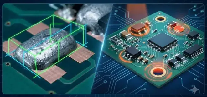
Solder paste deposition remains the single largest contributor to soldering defects. SPI systems measure volume, height, and area of every deposit immediately after printing. Volume deviations outside the process window—commonly set at ±25 % of nominal—trigger automatic stencil cleaning or printer adjustment before components are placed. Without SPI, insufficient paste produces open joints while excess paste creates bridges that AOI may later flag but cannot prevent.
Post-reflow AOI then examines the assembled board under multiple lighting angles and magnification levels. It detects tombstoning caused by uneven pad wetting, polarity reverses on diodes or polarized capacitors, and incomplete fillet formation. Modern systems also apply machine-learning classifiers trained on actual production defects rather than idealized CAD models, reducing false calls while maintaining high detection rates for true defects.
The combination of SPI and AOI creates a closed-loop feedback path: paste data informs printer maintenance schedules, and AOI defect maps guide placement machine calibration. Boards that pass both gates proceed with high confidence that visible and volumetric solder issues have been controlled.
Non-Destructive Verification of Hidden Joints via X-Ray Inspection
Surface inspection cannot evaluate the quality of solder joints beneath BGA, QFN, LGA, or press-fit connectors. X-ray systems, typically 2D or 3D computed tomography, quantify void percentage, bridge formation, and open joints inside these packages. IPC-A-610 and customer-specific criteria commonly limit total void area to 25–30 % for Class 2 and tighter limits for Class 3 or automotive applications.
Excessive voids under a BGA thermal pad reduce heat dissipation and create stress risers that propagate cracks during temperature cycling. Open joints on high-density QFN pads may pass functional test at room temperature yet fail under vibration or elevated temperature. X-ray therefore serves as the only practical non-destructive method to confirm joint integrity before boards leave the factory.
For high-reliability programs, sampling plans are replaced by 100 % X-ray on critical devices, with automated measurement of void size and location recorded for each serial number. This traceability supports root-cause analysis if field returns later occur.
Functional Testing and Final Validation for Mission-Critical Reliability
Electrical performance under actual operating conditions remains the final quality gate. In-circuit test, flying-probe, or functional test fixtures exercise power rails, signal paths, and communication interfaces. Boundary-scan techniques further verify interconnects that are inaccessible to probes.
Functional test catches issues that optical and X-ray methods miss: incorrect firmware loading, parametric drift outside specification, or intermittent contact caused by residual flux contamination. For medical and automotive PCBA, environmental stress screening—temperature cycling combined with power-on testing—may be added to precipitate latent defects before shipment.
Cost Escalation Risks When Inspection Stages Are Skipped
A missing or incomplete SPI check can allow an entire panel of boards with marginal paste deposits to enter reflow. Subsequent AOI will detect many of the resulting defects, yet the boards still require rework, additional X-ray, and retest. Industry data consistently show that the cost of correcting a defect rises by an order of magnitude at each successive process stage. Field failures multiply that cost further through warranty claims, line-down events at the customer, and potential regulatory scrutiny in safety-critical sectors.
Factories that maintain the full inspection sequence therefore treat early-stage process control as a cost-avoidance investment rather than an overhead. Yield data, scrap rates, and customer return metrics provide quantitative confirmation of the return on that investment.
Matching Inspection Methods to Component Types and Application Requirements
| Inspection Stage | Primary Defects Detected | Typical Coverage | Application Focus |
|---|---|---|---|
| Incoming Quality Control (IQC) | Counterfeit components, moisture damage, incorrect polarity, date-code non-compliance | 100 % visual + sampling electrical | All PCBA |
| First Article Inspection | Setup errors, stencil misalignment, incorrect BOM population | First panels of each run | New product introduction & process changes |
| Solder Paste Inspection (SPI) | Insufficient/excess volume, height variation, bridging risk | 100 % of deposits | Fine-pitch, high-density SMT |
| Automated Optical Inspection (AOI) | Tombstoning, polarity reverse, missing components, visible solder defects | 100 % of accessible surfaces | Post-reflow quality gate |
| X-Ray Inspection | Voids, opens, bridges under BGA/QFN/LGA | 100 % or sampling on hidden joints | High-reliability, automotive, medical |
| Functional / In-Circuit Test | Parametric failure, firmware error, intermittent opens | 100 % or statistical sample | Final electrical validation |
This matrix illustrates that no single method addresses every defect mechanism. Effective PCBA manufacturing therefore sequences complementary technologies so that each stage targets the failure modes most likely to appear at that point in the process.
FAQ
Q1: Why does PCBA manufacturing need so many inspection stages instead of just final testing?
A1: Multiple stages target specific defect types at the point they occur—material issues early, soldering defects mid-process, and functional performance at the end—preventing expensive rework and field failures that a single final inspection cannot catch.
Q2: When is X-ray inspection required in PCBA production?
A2: X-ray is typically required for components with hidden solder joints such as BGAs and QFNs, especially in high-reliability applications like aerospace, medical, or automotive electronics where surface inspection alone is insufficient.
Q3: How do inspection processes impact PCBA cost and lead time?
A3: While adding controlled steps, robust inspections reduce overall costs by minimizing scrap, rework, and warranty claims. For complex or high-volume projects, they are a standard part of professional PCBA services.
Q4: What DFM practices improve the effectiveness of AOI and X-ray inspection?
A4: Adequate component spacing, consistent pad geometries, and clear polarity markings reduce false calls in AOI. For X-ray, avoiding overlapping packages on opposite sides of the board and providing adequate thermal vias under BGA pads improve image clarity and void measurement accuracy. Designers who incorporate these rules early experience higher first-pass inspection yields.
Q5: Can SPI data be used to improve stencil design and printer setup?
A5: Yes. Trend analysis of SPI volume and height data identifies apertures that consistently deposit outside the process window. Adjustments to aperture wall angle, area ratio, or printer pressure and speed are then validated on subsequent panels, converting inspection results into permanent process improvements.
In electronics manufacturing, the most expensive defect isn't the one you find—it's the one you miss. A single issue caught early takes seconds to correct. The same defect discovered after shipment can cost thousands times more to fix. This is why modern PCBA production never relies on a single inspection at the end of the line. Instead, multiple inspection stages are built into the process, each designed to catch a different type of defect before it moves further downstream.
In this video, we'll walk through some of the most common inspection stages inside a PCBA factory and explain what each one is designed to prevent. Let's get started.
The first line of defense begins before a single automated machine turns on, targeting risks at the raw material stage. Incoming Quality Control verifies component-level integrity. By inspecting lead planarity and terminal finishes under magnification, technicians identify conditions that could compromise solderability later in the assembly process.
Before production starts, operators perform a final material verification check, comparing component reel labels against production records. This step ensures that every feeder position contains the exact component specified in the bill of materials, eliminating costly loading errors.
Following the setup, the line executes a First Article Inspection. Rather than checking individual materials, First Article Inspection verifies the entire automated configuration. Inspectors manually confirm the placement, value, and orientation on the first completed assembly. Only after the first article is approved is the line released for volume manufacturing.
With the setup validated, the substrate enters the active surface mount line. Many soldering defects can be traced back to issues during solder paste printing.The primary risk here is volume inconsistency: excess solder bridges during heating to cause short circuits, while insufficient paste results in fragile joints that crack under mechanical loads. To solve this, the SPI system projects structured light across the printed pads, measuring the exact height and volume of every deposit to intercept printing deviations before component placement occurs. After components are placed and the board passes through the reflow oven, the liquid alloy solidifies into permanent metallurgical bonds.
During this high-speed thermal cycle, components can shift, lift, or stand completely upright—a defect known as tombstoning. To capture these surface-level errors, the assembly enters the post-reflow AOI system. Using multi-directional LED illumination and high-resolution cameras, the AOI software automatically compares the geometric features of every component and solder fillet against an established standard, immediately flagging anomalies like missing parts or polarity reversals for technician review.
By this stage, most manufacturing defects have already been screened out. The remaining objective is to verify overall workmanship before shipment.After production is complete, every assembly undergoes a final quality inspection. Inspectors perform a visual audit to verify workmanship, cleanliness, component integrity, and any signs of handling damage before the product is approved for shipment.
Depending on the product's complexity and reliability requirements, additional verification methods may also be included as part of the manufacturing process.
Packages such as BGAs and QFNs hide their solder joints beneath the component body, making them impossible to evaluate with conventional optical systems. When customers require additional verification, the boards may undergo X-ray inspection. By penetrating the component package, the X-ray system reveals hidden solder connections and helps identify defects that cannot be detected from the surface.
Functional Testing provides another layer of validation. By powering the assembly and simulating real operating conditions, engineers can verify that key circuits, interfaces, and control functions behave as intended before shipment. The exact test procedure varies depending on the product and customer requirements.
No single inspection can catch every defect. Each checkpoint exists because it protects against a different type of failure. Some verify materials, some evaluate solder quality, and others confirm electrical performance. Together, these layers of verification transform a bare PCB and a collection of components into hardware that can be trusted in the real world.





