










One-Stop PCBA Video: End-to-End Precision from Prototype to Volume Production
Key Moment
What This Video Covers
This video explains AIVON's end-to-end one-stop PCBA capabilities, covering the complete journey from rapid prototyping through high-volume manufacturing. It highlights advanced SMT assembly lines, automated production processes, and rigorous quality control that includes AOI inspection, X-ray analysis, and full functional testing to ensure every board meets demanding real-world performance standards.
Viewers learn how AIVON combines fast turnaround times with scalable production capacity and full turnkey service, enabling engineering teams to move from design validation to global deployment with confidence. The content is especially relevant for professionals working on automotive electronics, medical devices, industrial control systems, and IoT applications where reliability and speed are critical.
For an instant quote on your next project, explore our PCB assembly quote tool or request a PCB prototype today.
Key Highlights
- Advanced SMT lines with automated production deliver consistent quality from prototype to high-volume runs
- Multi-stage inspection (AOI, X-ray, functional testing) ensures high-reliability boards for mission-critical applications
- Full turnkey PCBA service accelerates time-to-market while maintaining scalability and cost efficiency
Advanced SMT Lines and Automated Production for Consistent Yield
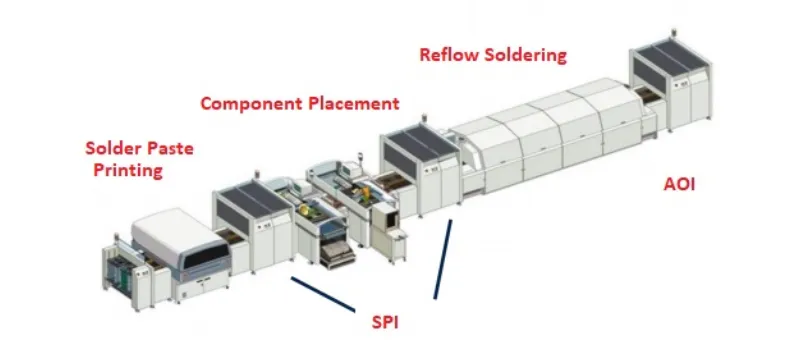
Modern one-stop PCBA relies on high-speed SMT lines equipped with precision pick-and-place systems, nitrogen reflow ovens, and closed-loop process controls. These lines maintain placement accuracy within ±25 µm and achieve first-pass yields above 98 % when designs follow standard DFM rules for component spacing, pad geometry, and thermal relief.
In real production, inconsistent paste volume or poorly optimized reflow profiles commonly cause tombstoning, bridging, or insufficient solder joints—especially on fine-pitch BGAs and 0201/01005 passives. Automated optical paste inspection and real-time SPI feedback correct these issues before placement, preventing downstream rework that can add 3–7 days to a schedule.
For volume runs, dual-lane or multi-line configurations allow simultaneous processing of mixed product families while maintaining traceability through barcode and MES integration. This capability is essential when automotive or medical customers require full lot control and process capability indices (Cpk > 1.33) on critical parameters such as solder joint voiding and shear strength.
Designers benefit from early DFM reviews that flag panelization inefficiencies, unsupported via-in-pad structures, or non-standard stencil apertures—issues that frequently reduce throughput by 15–25 % if left unaddressed until the pilot run.
Multi-Stage Inspection Ensuring Mission-Critical Reliability
AOI systems capture both 2D and 3D images after reflow to detect missing components, polarity errors, and solder defects at rates exceeding 10 000 components per hour. X-ray inspection then verifies hidden joints under BGAs, QFNs, and connectors, quantifying void percentages against IPC-A-610 and customer-specific limits (typically <25 % for automotive Class 3).
Functional testing closes the loop by exercising the board under simulated operating conditions—temperature cycling, voltage extremes, and communication protocols—before shipment. Boards that pass only visual or X-ray checks but fail functional test often reveal subtle issues such as cracked vias from CTE mismatch or insufficient conformal coating coverage.
Skipping any stage introduces measurable risk: industry data show that latent solder joint failures in automotive ECUs can exceed 200 ppm when X-ray is omitted, while medical devices face regulatory non-conformance if functional coverage falls below required test vectors. Integrating all three methods within a single one-stop flow eliminates hand-offs that historically caused 5–10 % of field returns.
Full Turnkey Service Accelerating Time-to-Market
True one-stop PCBA encompasses component procurement, kitting, SMT/through-hole assembly, conformal coating, programming, and final packaging under a single quality system. This eliminates the typical 2–3 week delay associated with coordinating separate fabricators, assemblers, and test houses.
Procurement teams gain leverage through consolidated BOM management and alternative-part qualification, reducing the impact of allocation shortages that frequently extend prototype cycles by 4–8 weeks. Engineering teams receive a single point of contact for ECO implementation, ensuring design changes propagate correctly across stencil, fixture, and test-program revisions without version mismatches.
Common Manufacturing Challenges in Scaling One-Stop PCBA
Transitioning from prototype to volume often exposes process windows that were acceptable at low volume but become unstable at scale. Examples include stencil aperture design that works for 50 boards yet produces insufficient paste volume on 5 000-board runs, or reflow profiles tuned for mixed technology that create excessive voids once panel size increases.
Component moisture sensitivity and bake requirements become critical when daily throughput rises; failure to control MSL levels leads to popcorning and delamination. Likewise, fixture wear and probe contamination in ICT or functional testers can degrade contact resistance after several hundred cycles if preventive maintenance is not scheduled.
These risks are mitigated by process capability studies performed during the pilot phase and by locking qualified parameter windows before volume release.
DFM Best Practices for Seamless Prototype-to-Volume Transition
Successful one-stop PCBA starts with design rules that align with the manufacturer’s process capability: minimum 0.1 mm solder-mask dam between pads, proper thermal relief on ground planes, and fiducial placement optimized for multi-panel arrays. Early submission of Gerber, BOM, and centroid data allows simultaneous DFM and DFA analysis, catching issues such as non-standard package outlines or unsupported via structures before tooling begins.
Panelization should maximize material utilization while maintaining adequate breakaway and tooling margins; improper panel design can reduce usable yield by 8–12 %. For high-reliability markets, specifying IPC Class 3 acceptance criteria and requiring X-ray void data on first-article reports provides objective evidence of process control.
| Process Stage | Typical Cycle Time (Prototype) | Typical Cycle Time (Volume) | Key DFM Risk if Overlooked | Recommended Control |
|---|---|---|---|---|
| Component Procurement | 5–10 days | 2–4 weeks (with buffer) | Allocation / counterfeit risk | AVL + incoming X-ray / electrical |
| SMT Assembly | 2–3 days | Continuous multi-line | Paste volume / reflow voids | SPI + 3D AOI + profile lock |
| Inspection & Test | 1–2 days | In-line + sampling | Hidden joint defects | 100 % AOI + X-ray + functional |
| Turnkey Packaging | 1 day | Same-day | Labeling / traceability errors | MES barcode + lot control |
FAQ
Q1: How quickly can AIVON complete high-volume PCBA production after prototype approval?
A1: AIVON typically transitions approved prototypes to high-volume PCBA within 2–4 weeks, depending on design complexity, component availability, and production schedule.
Q2: What inspection methods does AIVON use to guarantee reliability in automotive and medical PCBA?
A2: AIVON performs AOI (Automated Optical Inspection), X-ray inspection, and full functional testing on every production batch to meet strict automotive and medical reliability standards.
Q3: Does AIVON offer turnkey PCBA services that include component sourcing and final testing?
A3: Yes, AIVON provides complete turnkey PCBA services that cover component procurement, SMT assembly, and final functional testing.
Q4: What are the most common DFM issues that delay one-stop PCBA schedules?
A4: Frequent causes include insufficient pad-to-via clearance, non-optimized stencil apertures for fine-pitch devices, missing fiducials on multi-panel arrays, and BOMs containing obsolete or long-lead components. Addressing these during the design review stage typically recovers 1–2 weeks of schedule.
Q5: How does one-stop PCBA reduce risk compared with multi-vendor supply chains?
A5: Single-source accountability eliminates interface errors between fabrication, assembly, and test houses. Process parameters, material lots, and test data remain under one quality system, improving traceability and reducing the probability of mismatched revisions or incomplete test coverage.
Precision,Speed,Reliability. That's how modern PCBA should be built.
Whether you're launching a rapid prototype or scaling to global production, you need a partner who delivers precision — every single time.
At AIVON, we turn complexity into consistency.
Powered by 7 Siemens SMT lines and 10 high-precision placement machines, our fully automated production delivers exceptional speed and accuracy.
From SMT to THT, we support rigid, flex, and complex PCB designs — so you can build without constraints.
We don't just follow specs; we deliver full turnkey solutions that simplify your workflow and accelerate time to market.
Quality is at the heart of everything we do. Our technicians perform careful first-article verification, followed by 100% AOI and X-Ray inspection. Every board undergoes strict electrical and functional testing to guarantee the highest reliability.
With advanced facilities, powerful production capacity, versatile capabilities, and uncompromising quality control, AIVON is your reliable partner for turning ideas into reality.
Fast delivery. High reliability. One-stop solution.
Bring your PCB ideas to life with AIVON. Visit aivon.com today and get your instant quote. We're ready to build with you.





