Inside the Modern PCB Factory: From Design to High-Volume Production
WHAT THIS VIDEO COVERS
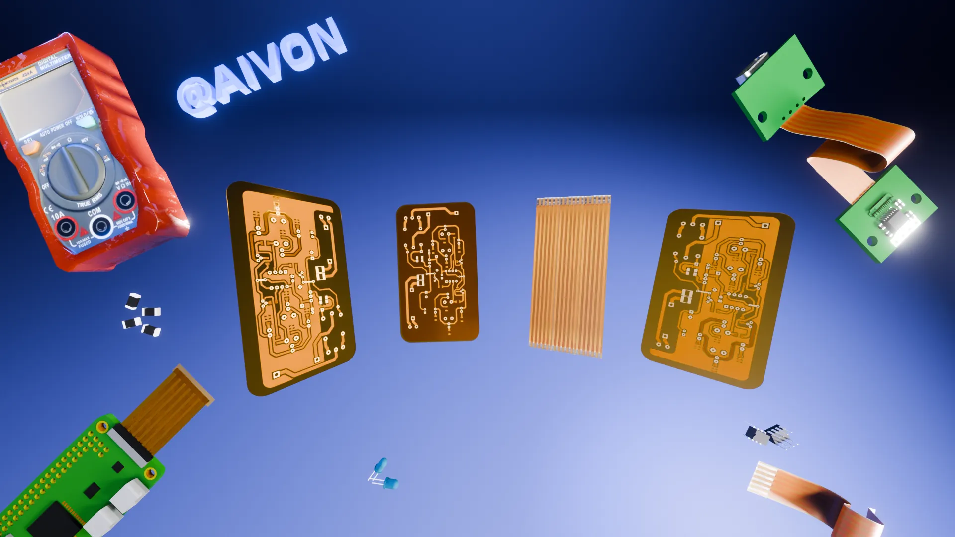
This video provides a clear, step-by-step tour inside a real high-volume PCB factory, showing the complete manufacturing journey from digital design files to fully functional boards ready for assembly. Viewers see every major fabrication stage with practical explanations, including material preparation, layer stack-up, drilling, plating, and final processing that ensure precision and consistency at scale.
The content highlights how modern factories support complex multilayer and high-reliability designs used in demanding environments. It is especially valuable for engineering and procurement teams working on automotive electronics, aerospace systems, electric vehicles, and industrial control applications where quality and volume are critical.
For immediate project support, request a PCB mass production quote or explore our automotive PCB capabilities.
KEY HIGHLIGHTS
- Complete PCB fabrication workflow from Gerber files to finished boards in a single high-volume facility
- Scalable manufacturing processes supporting multilayer, high-reliability designs for automotive and aerospace use
- Direct transition from prototype validation to mass production with consistent quality control
FAQ
Q1: How many layers can modern high-volume PCB factories reliably produce?
A1: Modern high-volume PCB factories routinely produce boards with 4 to 20+ layers while maintaining tight impedance control, high yield rates, and consistent quality across large production runs.
Q2: What are the critical steps shown in a real PCB manufacturing process from design to finished board?
A2: The complete process includes design file preparation, inner layer imaging, lamination, mechanical drilling, copper plating, outer layer etching, solder mask application, surface finish (ENIG or HASL), and final electrical testing.
Q3: How does high-volume PCB production differ from prototyping in terms of process and lead time?
A3: High-volume production uses optimized panelization, dedicated tooling, and automated lines for cost efficiency, typically achieving 2–5 week lead times compared to 3–10 days for prototype quantities.
Printed Circuit Boards, or PCBs, are the foundation of nearly every electronic device we use today — from your smartphone and laptop to electric vehicles and satellites. In this video, we're going to walk you through the complete PCB manufacturing process in under 7 minutes. From digital design files to a fully functional board ready for assembly, you'll see every major step in a real high-volume factory.
Step 1 DFM&Material Cutting
It all starts in the Engineering department. The factory receives your Gerber files, drill files, and BOM. Engineers run a Design for Manufacturability (DFM) check to verify trace widths, clearances, drill sizes, and layer stack-up are within the factory's capabilities.
Once approved, raw material preparation begins. Standard panels of FR-4 epoxy glass-fiber laminate (usually 1.6 mm thick with 1 oz or 2 oz copper foil) are cut into production-sized panels.Any rough edges are deburred to prevent defects downstream.
Step 2: Inner Layer Circuit Patterning
For multi layer boards — which make up most modern PCBs — inner layers are created first. The copper surface is cleaned and a thin photosensitive dry film is laminated on both sides. Using Laser Direct Imaging or UV exposure, the circuit pattern from your Gerber file is transferred onto the film. After development, the unwanted copper is chemically etched away in an alkaline solution, leaving only the protected circuit traces. The dry film is then stripped off. Finally, Automated Optical Inspection (AOI) scans every micron of the layer for shorts, opens, or defects. This step ensures the inner circuitry is flawless before layers are bonded together.
Step 3: Lamination & Pressing
Now the layers are fused into one solid board. First, the inner layers undergo brown oxide treatment to roughen the copper surface and improve adhesion. Then, in a cleanroom, Prepreg sheets are manually pre-stacked between the inner cores.After that, the panels enter a emi-automated stacking system, where copper foils are added on both sides to complete the full structure.Once assembled, the stack is transferred via conveyor directly into the lamination press.Inside, heat and pressure do the real work — typically around 180 to 200°C and over 300 psi.
The prepreg melts and flows, bonding everything into a single solid structure.What comes out is a rigid multilayer board — with each layer electrically isolated, but perfectly connected where it needs to be.
Step 4: Drilling & Plating Through Holes
Holes are next. Using ultra-precise CNC drills, thousands of vias are drilled exactly where needed for interlayer connections. After drilling, the panel goes through deburring and plasma desmear to clean the hole walls.
Then comes the critical electroless copper deposition — a chemical process that deposits a thin 0.5 to 1 micron layer of copper on the non-conductive hole walls. Finally, electrolytic plating thickens this copper to 15 to 25 microns, creating reliable conductive pathways between every layer. Without this step, multilayer boards simply wouldn't work.
Step 5: Outer Layer Circuit Patterning
Outer layers follow almost the same process as inner layers, but with one important difference. Dry film is applied again, the outer circuit pattern is imaged and developed, and then we do pattern plating: additional copper is electroplated only where needed, followed by a thin tin layer that acts as an etch resist. The unwanted copper is etched away, and the tin is later stripped off. This leaves clean, raised copper traces on the outer surfaces, protected and ready for soldering. AOI checks the outer layers just like the inner ones.
Step 6: Solder Mask & Silkscreen
To protect the copper and prevent solder bridges during assembly, a liquid photo-imageable solder mask (usually green epoxy) is applied over the entire board. It's exposed and developed to open up only the pads and vias that need to be soldered. After curing under UV light, the board gets its professional look. Next, white legend or silkscreen ink is printed to add component designators, polarity marks, logos, and assembly notes. A final cure hardens everything. This step not only protects the board but makes it easy for technicians to assemble.
Step 7: Surface Finish & Electrical Testing
Surface finish is crucial for solderability and oxidation protection. Options like ENIG, HASL, or OSP are applied only to the exposed copper pads. Immediately following this, every board undergoes 100% electrical testing. We use flying probes for prototypes or dedicated test fixtures for volume production to verify continuity and isolation on every net. This ensures the board is electrically perfect before it moves to final shaping.
Step 8: Profiling, Final Inspection & Packaging
Once electrical integrity is confirmed, the panel is profiled. CNC routers or V-scoring machines cut the large panel into individual boards, adding any required slots or bevels. Finally, our team performs a manual final inspection alongside AOI to catch any cosmetic or dimensional issues. Only flawless boards are vacuum-packed with desiccant, labeled, and shipped to customers worldwide.
That's the complete journey — over 200 highly automated steps, extreme precision down to 50 microns, and strict environmental controls for wastewater and chemicals. AivonPCB factories produce hundreds of thousands of boards every day with incredible reliability.
If you're designing your next project or just love tech, drop a comment: which step surprised you the most? Like, subscribe, and hit the bell for more deep-dive electronics videos — next up, we'll cover SMT assembly!