










How Signals Jump Between PCB Layers: Vias Explained
WHAT THIS VIDEO COVERS
This video clearly explains how electrical signals move between different layers in a multilayer PCB using vias - the plated holes that form vertical interconnections in the layer stack-up.
It covers the four main via types: through-hole vias, blind vias, buried vias, and microvias. You'll learn their construction methods (drilling, plating, and lamination sequencing), key performance characteristics such as inductance, signal path length, and routing density impact, plus real manufacturing considerations including cost and complexity.
Shorter vias (especially microvias in HDI PCB designs) deliver better high-speed performance and signal integrity, while through-hole vias remain the most economical and robust option for many applications. The video also touches on advanced variants like via-in-pad and back-drilled vias.
Understanding via selection directly affects board reliability, thermal management, and overall cost in demanding sectors such as aerospace, medical devices, automotive electronics, and high-frequency communication systems.
Get an instant PCB quote or explore our HDI PCB capabilities for advanced via technologies. For rigid-flex projects requiring complex via structures, see our rigid-flex PCB solutions.
KEY HIGHLIGHTS
- Through-hole vias offer the simplest and most cost-effective vertical connection but consume routing space on every layer they penetrate.
- Blind and buried vias improve routing density and signal integrity by connecting only specific layers, though they require precise depth control and additional manufacturing steps.
- Microvias (laser-drilled, <150 μm) are essential for HDI boards, delivering lower inductance and superior high-speed performance at higher cost.
How Vias Enable Vertical Signal Transmission in Multilayer PCBs
In multilayer PCBs, signals travel horizontally along copper traces on individual layers and vertically through vias to complete circuits across the stack-up. Vias are copper-plated holes that provide these interlayer connections, ensuring continuity in complex designs with four or more layers.
During fabrication, vias are formed after initial lamination or at specific stages depending on type. The plating process deposits conductive copper on the hole walls, creating a reliable electrical path. In high-layer-count boards, proper via placement is critical to avoid signal reflections, crosstalk, and impedance discontinuities.
From a manufacturing perspective, via aspect ratio (depth to diameter) directly influences plating quality. High aspect ratios in through-hole vias can lead to uneven plating and potential voids if not controlled. Designers should maintain aspect ratios below 10:1 for standard through-hole vias to ensure reliable copper deposition and long-term reliability.
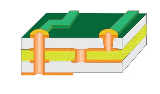
Key Via Types: Through-Hole, Blind, Buried, and Microvias Compared
| Via Type | Diameter Range | Layers Connected | Key Advantages | Manufacturing Complexity | Typical Applications |
|---|---|---|---|---|---|
| Through-Hole | 0.2–0.5 mm | All layers | Lowest cost, high reliability | Low | Standard multilayer boards |
| Blind | 0.1–0.3 mm | Outer to inner | Improved density, shorter paths | Medium-High | HDI, compact consumer electronics |
| Buried | 0.1–0.3 mm | Inner layers | Maximum routing density | High | High-speed servers, telecom |
| Microvia | <0.15 mm | 1–2 layers | Lowest inductance, HDI enablement | Very High (laser drill) | Smartphones, wearables, 5G |
Manufacturing Processes for Reliable Via Formation
Through-hole vias are typically mechanically drilled through the entire panel after full lamination, followed by desmear, electroless copper seeding, and electrolytic plating. Blind vias are drilled to a controlled depth before or during sequential lamination, requiring precise laser or mechanical control to avoid damaging underlying layers.
Buried vias are formed on inner layer cores before outer lamination, adding steps to the process flow. Microvias rely on CO2 or UV laser drilling for small diameters, often in stacked or staggered configurations for HDI builds. Each additional via type increases the number of lamination and drilling cycles, impacting yield and lead time.
In production, panelization and registration accuracy are vital. Misalignment during sequential lamination can cause via-to-trace shorts or open circuits. Factories often use X-ray inspection or automated optical inspection (AOI) to verify via quality post-plating.
Signal Integrity and Electrical Performance Impacts of Via Selection
Shorter vias reduce parasitic inductance and capacitance, minimizing signal degradation in high-frequency applications. Through-hole vias create longer stubs that can act as antennas, causing resonances and reflections above several GHz. Back-drilling removes these stubs but adds cost.
Blind and buried vias shorten the signal path, improving impedance control and reducing crosstalk. Microvias excel in HDI designs due to their small size and ability to be placed in-pad, preserving routing channels. In practice, improper via selection in high-speed designs often leads to eye diagram closure and bit error rate issues during validation testing.
DFM Guidelines and Cost Considerations for Via Implementation
Designers should specify via types early and consult fabricators on capabilities. For example, minimum annular ring sizes must account for drill wander and plating tolerances. Overly aggressive microvia stacking without adequate resin fill can cause delamination under thermal stress.
Cost escalates significantly with blind/buried and laser-drilled vias due to extra process steps and lower panel utilization. A balanced approach—using through-hole vias for power/ground and advanced vias only for critical signals—optimizes both performance and manufacturability.
Common risks include via barrel cracking from CTE mismatch in lead-free soldering and insufficient plating thickness leading to opens after thermal cycling. Following IPC standards and providing clear stack-up drawings helps mitigate these issues.
Common Via-Related Manufacturing Defects and Prevention Strategies
Typical defects include plating voids, resin smear in drilled holes, and breakout where vias intersect traces too close to the edge. Prevention starts with proper material selection (e.g., low-Dk laminates for high-speed) and controlled drilling parameters.
For HDI boards, sequential lamination with filled microvias reduces reliability risks compared to unfilled ones. Thermal management is also key—vias can serve dual purposes as heat conduits when filled with conductive material.
Engineers should review DFM reports for via-specific flags such as aspect ratio violations or insufficient clearance to copper features.
FAQ
Q1: When should I use blind or buried vias instead of through-hole vias?
A1: Use blind or buried vias when you need higher routing density, shorter signal paths, or better signal integrity in compact multilayer designs. They increase cost and complexity, so they are justified primarily in HDI, high-speed, or space-constrained applications.
Q2: What are microvias and why are they important for modern PCBs?
A2: Microvias are tiny laser-drilled holes (usually under 150 μm) used in HDI PCBs. They enable higher layer counts and better electrical performance by reducing inductance and allowing stacked or staggered configurations critical for high-frequency and dense electronics.
Q3: How do vias affect PCB cost and manufacturing?
A3: More advanced vias (blind, buried, microvias) significantly raise fabrication cost due to extra drilling, plating, and lamination steps. Designers must balance performance needs against budget - using high-end vias only where they deliver clear value.
Q4: What is via-in-pad technology and when is it recommended?
A4: Via-in-pad places microvias directly under surface-mount pads, freeing routing space and improving thermal/electrical performance for BGA and QFN packages. It requires via filling and capping to ensure flatness for soldering. Recommended for high-density designs but increases cost and demands excellent registration accuracy to prevent solder wicking issues.
Q5: How can back-drilling improve high-speed PCB performance?
A5: Back-drilling removes the unused via stub after plating, reducing signal reflections and improving impedance matching in multi-GHz applications. This extra step is common in telecom and server boards. It requires precise depth control to avoid damaging active layers and is best specified clearly in fabrication notes.
Ever wonder how signals travel between PCB layers?
They go through tiny copper holes — called vias!
A through-hole via drills through every layer.
It's plated with copper along the wall, forming a solid connection.
It cheap and robust — but it wastes routing space on every layer it passes.
A blind via connects an outer layer to inner ones.
It shortens signal paths and frees routing channels below.
But it needs precise depth control.
A buried via hides completely inside inner layers.
It saves outer space,but it must be made before final lamination, increasing process steps and cost.
Microvias are laser-drilled, tiny — usually under 150 μm.
They're used in HDI boards, stacked or staggered between layers.
Shorter vias mean lower inductance and better high-speed performance.
but the higher the cost and complexity.
There are also back-drilled, via-in-pad, and stacked vias——more advanced forms we'll cover later.
Always balance performance, density, and bud get —use the smallest via only when it truly helps,not just because it looks high-end.





