 00:54
00:54
Via Types
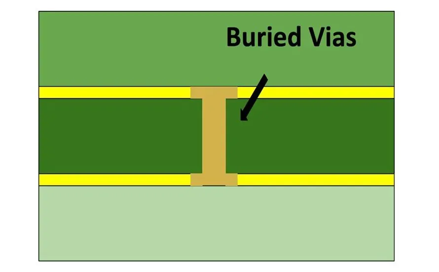
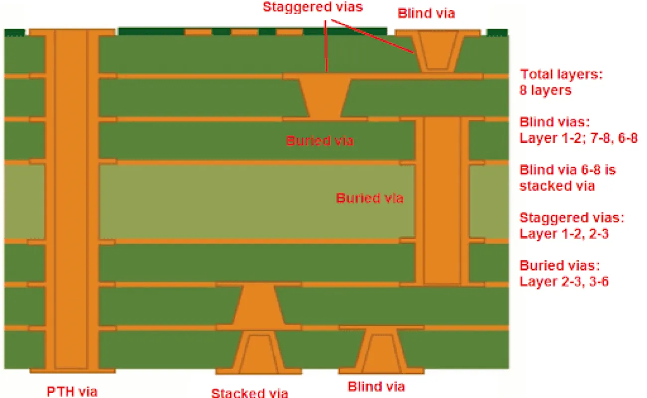
Vias play a critical role in printed circuit board (PCB) design, enabling electrical connections between multiple layers to ensure efficient signal routing and power distribution. Understanding the various via types is essential for engineers, designers, and hobbyists aiming to optimize board performance, minimize signal interference, and reduce manufacturing costs. This tag page on Via Types gathers in-depth articles that explore the fundamentals, from basic through-hole vias to advanced options like blind, buried, and microvias, helping you select the right approach for your specific project needs. For those searching for information on via types, the content here addresses key considerations such as thermal management, high-density interconnects, and reliability in high-speed applications. Through-hole vias, for instance, provide robust mechanical strength and are ideal for prototypes or boards requiring easy repairs, while blind vias save space by connecting only certain layers without penetrating the entire board. Buried vias, hidden within internal layers, support complex multilayer designs without affecting outer surfaces, and microvias enable finer pitches in compact electronics like smartphones and wearables. Best practices include evaluating via aspect ratios to prevent plating issues, incorporating via stitching for ground planes to enhance EMI shielding, and using simulation tools to predict signal integrity before fabrication. By delving into these articles, you can gain actionable insights into implementing via types effectively, whether troubleshooting common defects like via tenting or scaling up for production. This knowledge empowers you to make informed decisions that improve PCB functionality and longevity, drawing from real-world examples and expert analyses shared across our technical resources.
Video Guide



Technical Articles
Via Design Guidelines in PCB Design: Balancing Performance and Cost
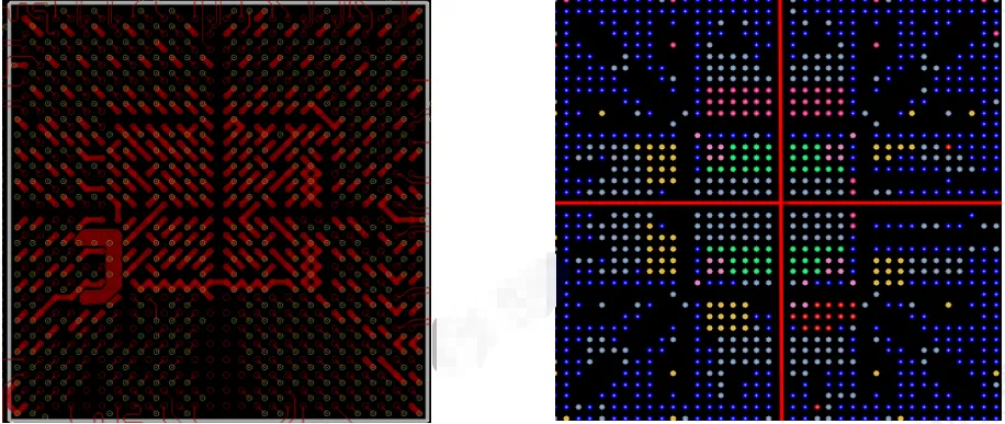
PCB Via Fanout Details That Are Easy to Miss
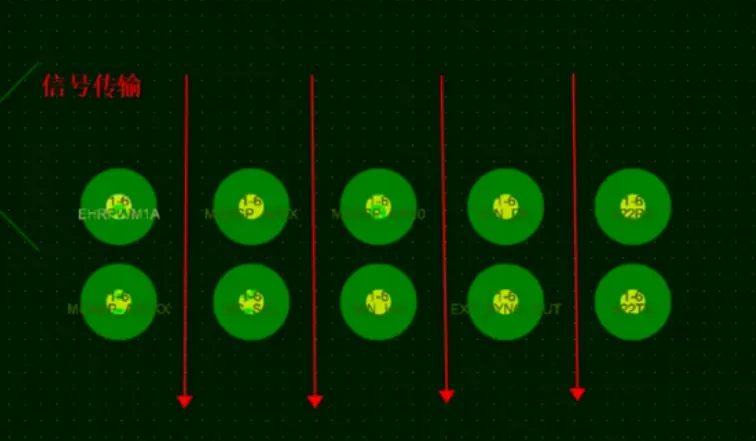
High-Speed PCB Vias: A Small Feature That Can Break the Signal
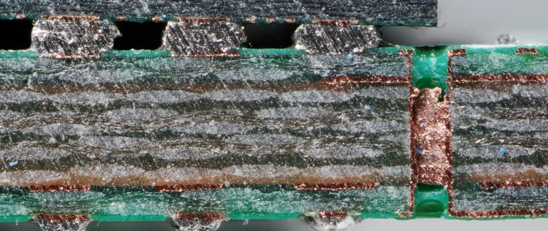
Small Anti-Pads Can Cause Unconnected Vias to Short
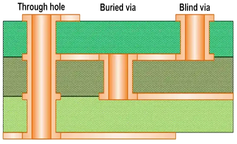
Cost Effective Buried Via Implementation: Balancing Performance and Price
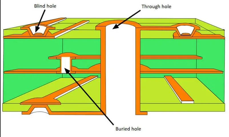
Mastering Via Design in Multilayer PCBs: A Comprehensive Guide
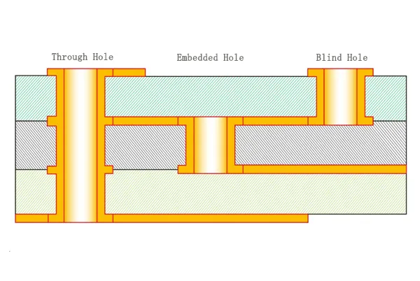
Optimizing Via Design in Rigid Flex PCBs: Enhancing Electrical and Mechanical Performance
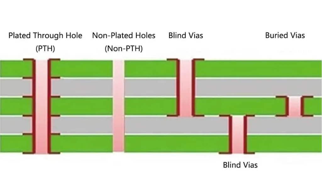
A Practical Guide to Selecting PCB Vias for Multilayer Designs
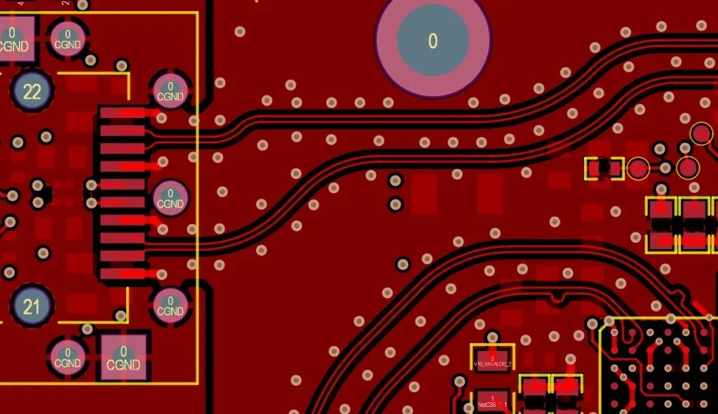
Via Strategies for High Density Double Layer PCBs: Types and Placement
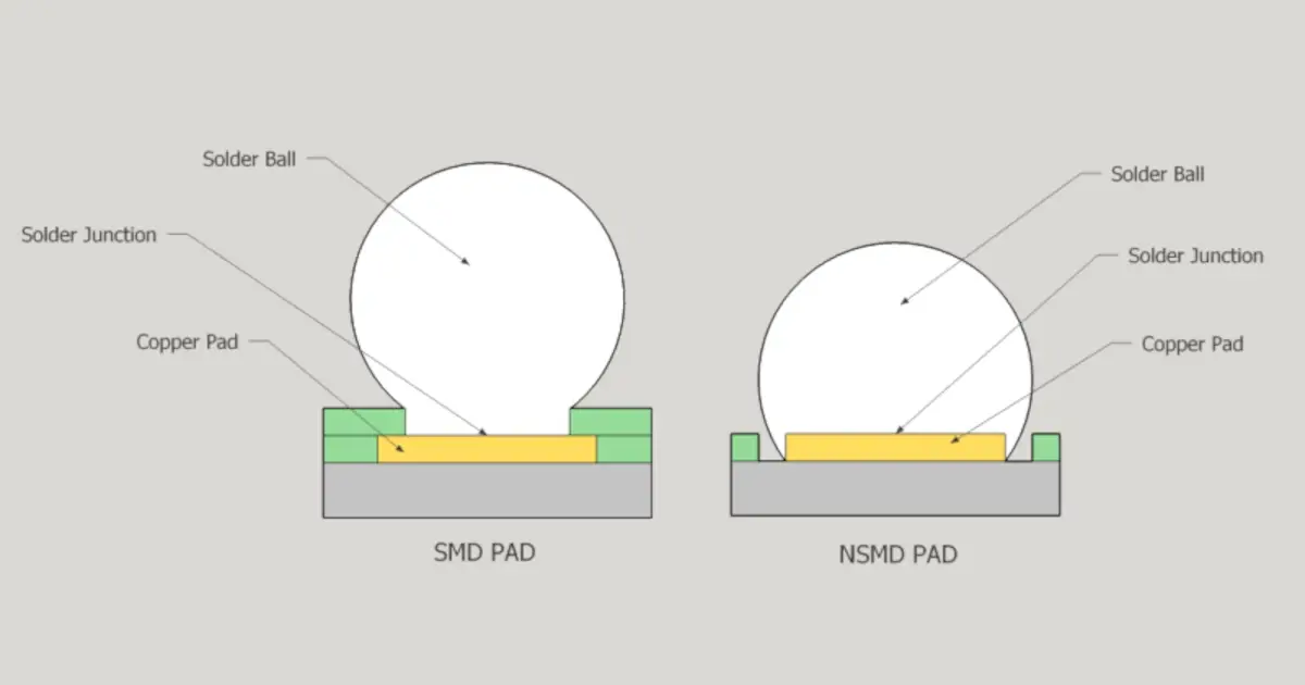
Fanout and routing: How to connect BGA packages to the rest of the PCB
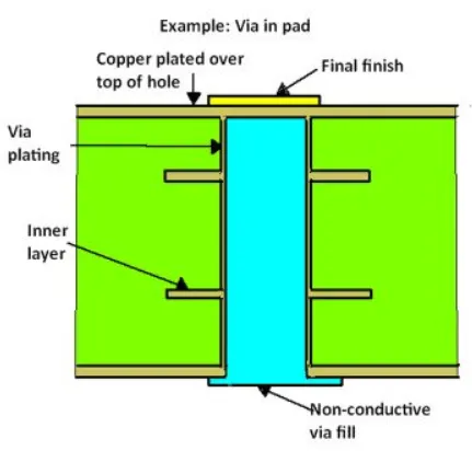
Via in Pad Alternatives: When to Choose a Different Via Structure
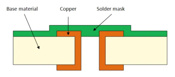
PCB via Plating: A Comprehensive Guide
Through-Hole Vias: Essential Connections in Multilayer PCB Design
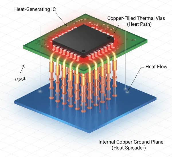
Enhancing PCB Reliability: A Guide to Thermal Vias for Heat Dissipation
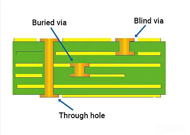
FR 4 PCB Vias: Types, Design Rules, and Manufacturing Considerations
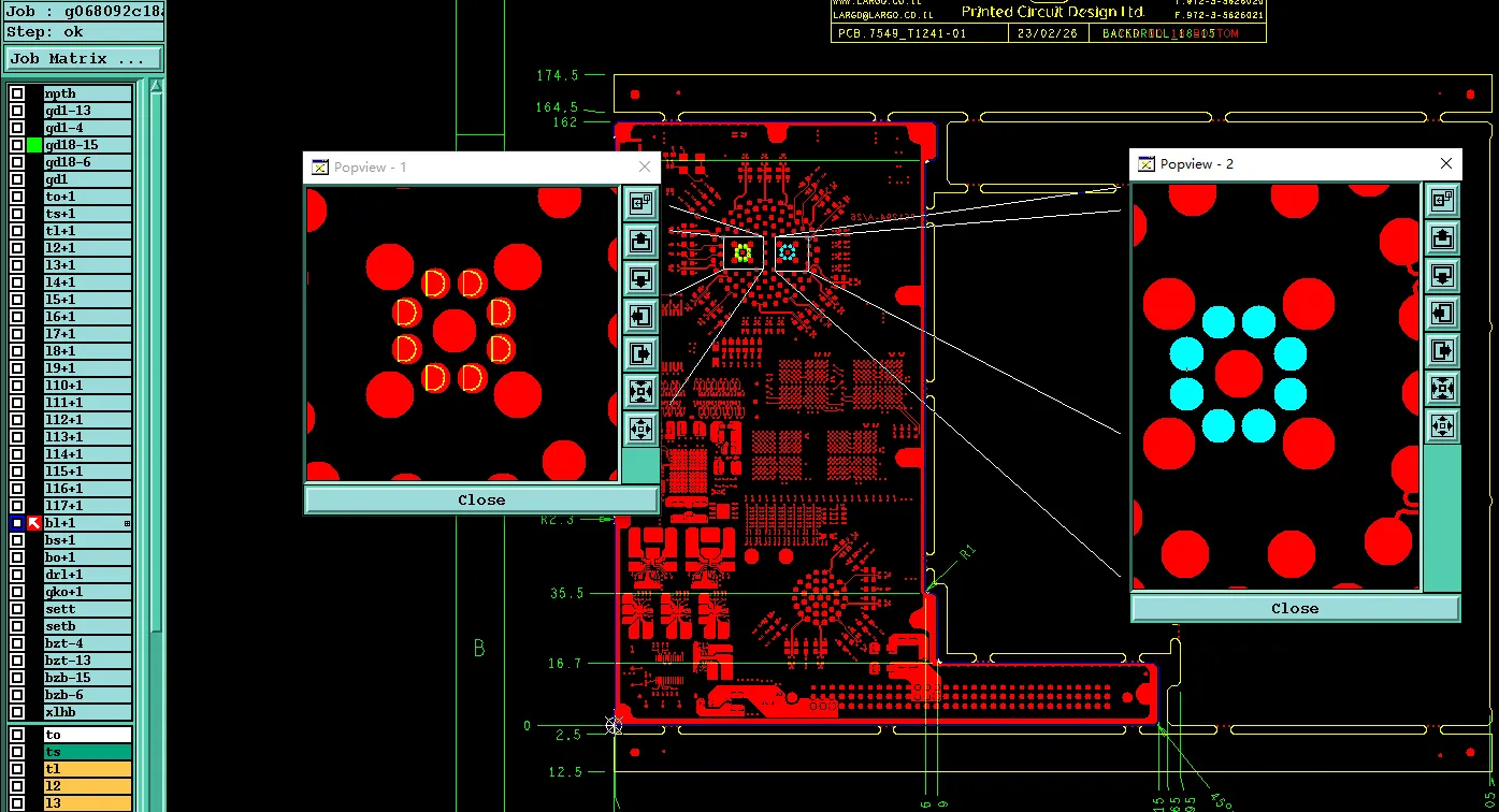
PCB Hole Attributes and Special Drilling: Common CAM Review Conflicts
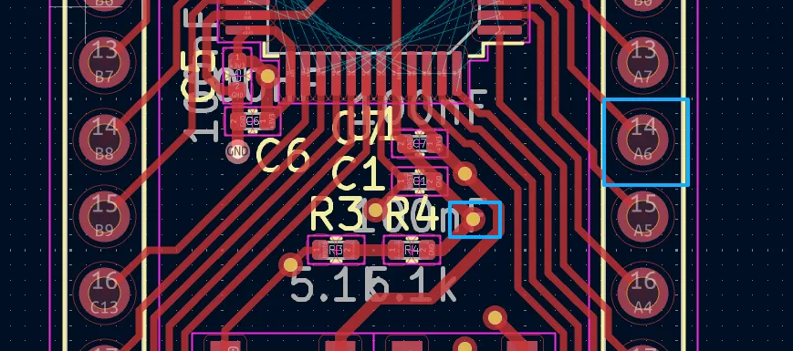
Via Design Guidelines for KiCad PCBs: Types, Rules and Manufacturing Considerations
Controlled Depth Drilling vs. Other Via Techniques: Choosing the Right Approach