










Via Tenting vs Resin Plugging: When Do You Need Resin Filling for Via-in-Pad Designs?
What This Video Covers
This video clarifies the practical difference between via tenting and resin plugging and shows engineers exactly when resin filling becomes necessary. Via tenting simply covers the via opening with solder mask. Resin plugging completely fills the barrel with epoxy resin, which is then cured and planarized. The critical use case is Via-in-Pad (VIP) construction, commonly required under high-density BGA and CSP packages. During reflow, molten solder can wick into an open via, starving the joint and creating reliability failures. Resin plugging blocks that path. The video also stresses that not every via on a board with BGA packages needs filling—if the via sits outside the pad and creates no soldering risk, standard tenting or open via treatment is usually acceptable. Selection must follow your design rules and the manufacturer's DFM capability. For dense multilayer or HDI PCB layouts that incorporate Via-in-Pad, early process confirmation is essential. Teams preparing PCB assembly or evaluating PCB prototype runs can use this distinction to avoid both over-specification and field failures.
Key Highlights
- Via tenting covers the opening with solder mask; resin plugging fully fills and cures the via barrel—two different processes with different process costs and planarity outcomes.
- Resin plugging is primarily required for Via-in-Pad designs under BGA/CSP packages to stop solder wicking during reflow and maintain joint volume.
- Not every via on a BGA board needs resin fill; vias located away from component pads can often remain tented if they introduce no soldering or reliability risk.
Via Tenting vs Resin Plugging – Core Process Differences
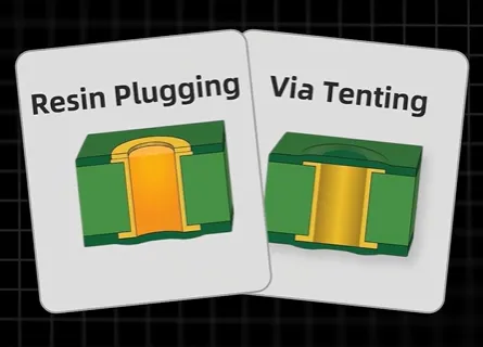
Via tenting is a solder-mask process. After plating, the solder-mask artwork is designed to cover the via openings on one or both sides. The mask is applied, exposed, and developed so that a continuous film of mask bridges the via. No material is introduced into the barrel itself. This is the lowest-cost and most common treatment for non-critical vias.
Resin plugging (also called via filling or via plugging) is a multi-step fabrication sequence. After drilling and plating, the vias are filled with a specialized epoxy resin, vacuum-assisted or screen-printed to remove voids. The resin is then cured, excess material is planarized by grinding or brushing, and the surface is prepared for subsequent plating or solder-mask application. The result is a solid, planar via that can accept copper plating over the top (plated-over filled via) or remain under solder mask.
These two processes differ in cost, cycle time, surface planarity, and suitability for fine-pitch SMT. Resin plugging adds process steps and material cost but delivers the mechanical and soldering reliability required for Via-in-Pad and certain high-reliability constructions.
When Resin Plugging Is Required for Via-in-Pad and BGA Packages
Via-in-Pad places the via directly inside the component land. This is common on HDI PCB and high-layer-count boards where routing density under BGA or CSP packages leaves no escape channels outside the pad. During SMT reflow the molten solder volume is limited. An open or only-tented via acts as a capillary path; solder is drawn into the barrel, leaving insufficient solder for a reliable joint. The result can be open joints, voids, or latent failures under thermal cycling.
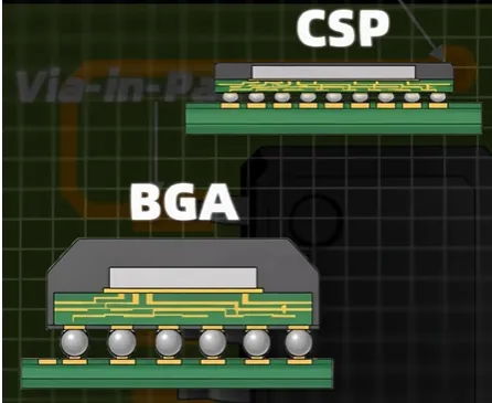
Resin plugging closes that path. Once the via is solidly filled and planarized, the pad surface behaves like a solid land. Solder stays on the pad, joint volume is controlled, and subsequent underfill or conformal coating processes are more predictable. This is especially important for fine-pitch BGAs (0.4 mm and below), CSPs, and any package where the via diameter is a significant fraction of the pad size.
However, the presence of a BGA package does not automatically require every via on the board to be resin-filled. Vias that are fully outside component pads, or that serve only as thermal or stitching vias with no soldering exposure, can usually remain tented or even open, provided the manufacturer's solder-mask tenting capability meets the design's hole-size and aspect-ratio limits. Over-specifying resin fill on non-critical vias increases cost and lead time without improving reliability.
DFM Selection Guide: Tenting or Resin Plug?
Use the following decision framework when releasing Gerber or ODB++ data:
| Design Condition | Recommended Treatment | Primary Reason | Typical Cost Impact |
|---|---|---|---|
| Via inside BGA/CSP pad (Via-in-Pad) | Resin plug + planarize | Prevents solder wicking and maintains joint volume | Highest |
| Via under QFN/LGA thermal pad | Resin plug (or copper fill) recommended | Thermal and solder control | High |
| Via outside component pads, no soldering risk | Solder-mask tenting | Lowest cost, adequate for most signal vias | Baseline |
| High-aspect-ratio vias (>8:1) or large via diameters | Confirm tenting capability; resin plug if tenting fails | Tenting reliability drops with diameter and aspect ratio | Medium |
| Boards requiring plated-over filled vias (POFV) for sequential lamination | Resin plug + copper cap | Enables reliable microvia stacking on HDI | Highest |
Always request the fabricator's current capability table for maximum tentable hole size, minimum resin-fill diameter, and planarity tolerance. Early DFM review prevents both unnecessary cost and late-stage process changes.
Key Manufacturing Risks and Factory Recommendations
The most frequent field failures linked to incorrect via treatment are solder starvation on Via-in-Pad joints and solder-mask tenting cracks that allow flux or moisture ingress. On the process side, incomplete resin fill leaves voids that can expand during reflow or thermal cycling, while over-aggressive planarization can thin the copper or damage surrounding pads.
Factory best practice is to declare Via-in-Pad locations explicitly in the fabrication notes and to specify "resin filled and planarized" rather than the ambiguous term "plugged." For tented vias, state the maximum allowable tented diameter and whether single-side or double-side tenting is required. When the design mixes both treatments on the same board, the fabricator must sequence the processes correctly—resin fill and planarization occur before final solder-mask application.
For high-reliability sectors (automotive electronics, medical devices, industrial control), many OEMs now default to resin-filled Via-in-Pad under all BGA packages and accept the cost trade-off for improved first-pass yield and long-term reliability. Prototype and low-volume runs can sometimes use selective tenting, but the same design rules should be validated before volume release.
FAQ
Q1: When is resin plugging mandatory for BGA packages?
A1: Resin plugging is required whenever a via is located inside a BGA or CSP pad (Via-in-Pad). Without the fill, solder can wick into the via during reflow, reducing joint volume and creating reliability risk. Vias outside the pads can usually remain tented.
Q2: Does every via on a board that contains a BGA need to be resin filled?
A2: No. Only vias that sit inside component pads or create a direct soldering risk need resin fill. Peripheral or stitching vias that do not intersect pads can normally use standard solder-mask tenting, reducing cost.
Q3: What is the main manufacturing difference between via tenting and resin plugging?
A3: Tenting is a solder-mask covering process that leaves the via barrel hollow. Resin plugging fills the barrel with epoxy, cures it, and planarizes the surface. The latter adds process steps, material cost, and enables plated-over filled vias for HDI stacking.
Q4: Can tenting fail on larger or high-aspect-ratio vias?
A4: Yes. Solder-mask tenting reliability decreases as via diameter increases and as aspect ratio rises. Most fabricators publish a maximum tentable hole size; beyond that limit resin plugging or other treatments become necessary.
Q5: How should Via-in-Pad requirements be specified to the PCB manufacturer?
A5: Clearly mark Via-in-Pad locations and state "resin filled, planarized, and copper capped if required." Supply the fabricator's DFM checklist early so process capability and cost can be confirmed before tooling.
Confused about via tenting and resin plugging?
Let's clear it up in one minute.
Look at these two vias.
Via tenting covers the via opening with solder mask, while resin plugging fills the via with resin and cures it.
So when do you need resin plugging?
One common case is Via-in-Pad, where a via sits directly inside a component pad.
This is often used in high-density packages like BGA and CSP.
Why fill the via?
During reflow, solder can flow into an open via, reducing the solder available for the joint.
Resin filling helps prevent this.
But having a BGA doesn't mean every via needs to be filled.
If the via is away from the pad and doesn't create a soldering risk, standard via treatment may be enough.
Tenting covers the opening.
Resin plugging fills the via.
Choose based on your design and manufacturer's DFM.





