










A recent 4-layer FR4 order arrived with clear production parameters: 101.6 mm × 101.6 mm outline, 2.4 mm finished thickness, TG150 material, 1 oz inner / 2 oz outer copper, lead-free HASL, green solder mask on both sides, and white silkscreen. Quantity was only five pieces, yet the design still required careful review before release. The customer specified via tenting (solder mask covering the vias) and provided a preferred stackup structure. Our engineering team examined the Gerber data against these requirements and immediately raised several Engineering Questions. The goal was not to delay the order but to prevent manufacturability problems that could reduce yield or affect long-term reliability.
From a DFM perspective, small quantity does not lower the risk threshold. A board that ships with unclear via covering or illegible markings can still create assembly defects, inspection failures, or field reliability issues. This order ( #FR4-20260411-036 ) shows how early clarification of via tenting, stackup, and silkscreen details protected both yield and product quality.
Why 2.4 mm Thickness and Mixed Via Data Required Immediate CAM Review
Several indicators flagged the need for thorough review. Board thickness of 2.4 mm on a 4-layer construction is thicker than the common 1.6 mm baseline. Material was specified as FR-4 Jian Tao (KB-6165F) with TG150. The customer also supplied a preferred stackup drawing. When the actual available core and prepreg combinations were compared with that drawing, dimensional and dielectric adjustments became necessary. At the same time, the fabrication notes called for full via tenting, yet the solder mask layers in the data showed mixed coverage—one side tented and the opposite side opened.
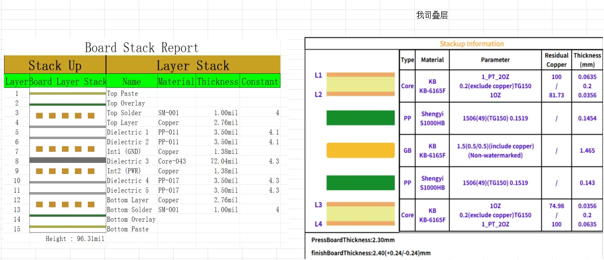
Figure 1: adjust stackup a little as the actual material as shown in the right of the attached picture
Silkscreen data contained characters whose line width fell below 5 mil and whose height fell below 30 mil. Hole size was listed at 0.3 mm with 18 µm finished copper plating, and the panel used V-cut separation with 4 mm process edges. None of these parameters were extreme on their own, but the combination of thickness, copper weight, mixed via treatment, and undersized legend created multiple points where manufacturing assumptions could diverge from design intent.
Our CAM engineer therefore treated the file as a risk-prevention exercise rather than a simple data-check. The primary concern was manufacturing stability across the entire process flow—from lamination through surface finish and final inspection.
Via Tenting Mismatch, Stackup Adjustment, and Silkscreen Limits
Three issues stood out by severity.
First, the via covering mismatch. The order clearly requested via tenting with solder mask. In the supplied Gerber files, however, many vias appeared tented on one side and left open on the opposite side. This mixed condition is common when a designer intends partial tenting for thermal or inspection reasons, yet it directly contradicts a full-cover requirement. From a process standpoint, the solder mask department would have to decide which data layer to follow. Any inconsistency risks incomplete coverage, mask residue inside the hole, or exposed copper at the via rim.
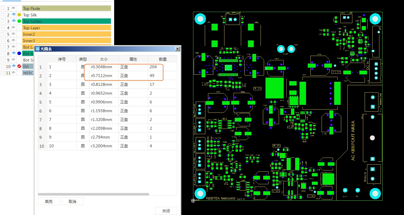
Figure 2: vias tenting for this order, but in the file, the vias are one side tenting and another side is solder mask opening
Second, the stackup required adjustment. The customer drawing defined a specific sequence of cores and prepregs to reach 2.4 mm. When matched against the actual KB-6165F material available in stock, the dielectric thicknesses and copper foil weights needed minor revision to stay within the ordered finished thickness and to maintain copper balance. Leaving the original stackup unchanged would have produced a board either over or under the 2.4 mm target, or would have forced non-standard pressing cycles that increase warpage risk on a thick 4-layer panel.
Third, silkscreen legibility. Character stroke width under 5 mil and height under 30 mil fall below the practical limit for reliable screen printing or inkjet legend on FR4. At these dimensions the ink tends to break up or spread, producing incomplete or blurred markings. On a board that carries white legend on green mask, poor clarity can hinder incoming inspection and later assembly identification.
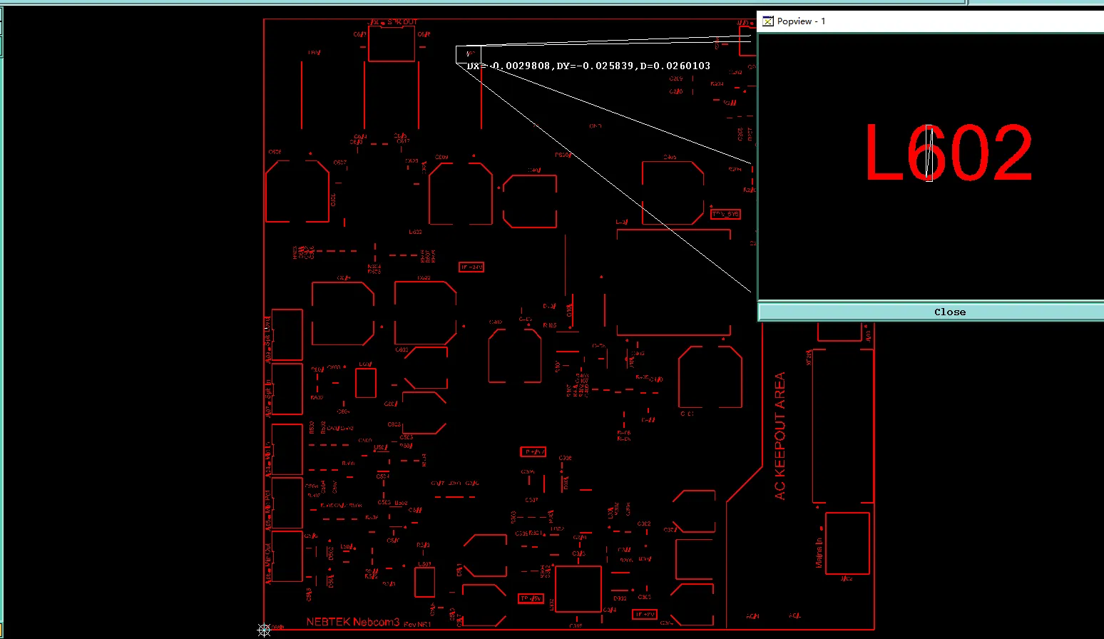
Figure 3: the legends in the original file have trace width of less than 5 mils and height of less than 30 mils
A secondary question concerned a pair of pads connected by a short trace: whether they belonged to the same electrical network. This point was less urgent than the three above, yet still required confirmation to avoid accidental net merging or isolation during CAM editing.
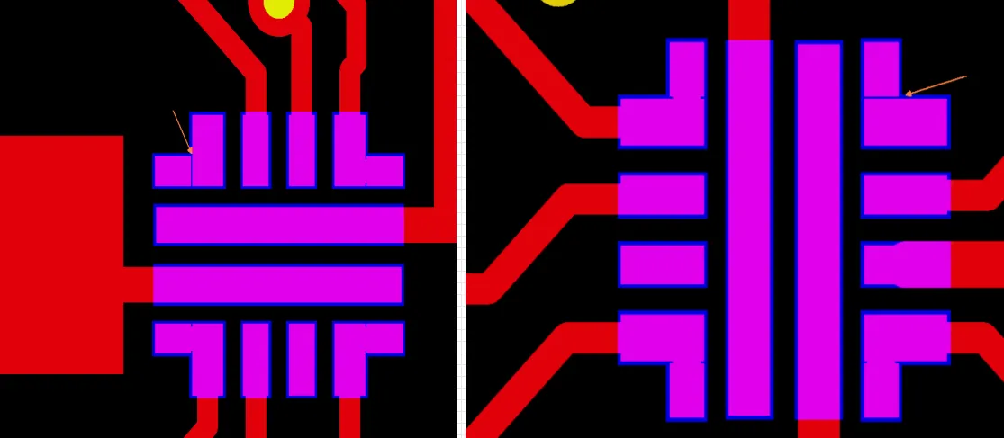
Figure 4: the track pads indicated by the arrows
| Risk Area | Observed Condition | Severity |
|---|---|---|
| Via tenting | Order requires full cover; data shows one-side open | High – process conflict |
| Stackup | Customer drawing vs. available KB-6165F material | High – thickness & balance |
| Silkscreen | Line width <5 mil, height <30 mil | Medium – readability |
| Net connectivity | Ambiguous pad pair | Low – confirmation only |
Table 1. Risk ranking used during the DFM review.
How Unresolved Via and Stackup Issues Could Affect Yield
If production had continued without clarifying the via tenting, two realistic outcomes were possible. Operators might have followed the order note and forced full tenting on both sides, covering the openings that the designer had left exposed. Conversely, they might have followed the Gerber data and left one side open. Either choice creates downstream problems. Open vias can allow solder to wick into the barrel during HASL or later assembly, producing voids or incomplete barrel fill. Residual flux trapped inside an open via is difficult to clean and can promote corrosion over time. Incomplete tenting can also leave thin mask bridges that crack under thermal stress, exposing copper at the via rim—an IPC-A-600 Class 2 concern for exposed copper near holes.
On the stackup side, forcing the customer's original dielectric sequence onto available KB-6165F stock risked finished thickness outside the ±10 % tolerance common for 2.4 mm boards. Uneven copper distribution between the 1 oz inner and 2 oz outer layers already requires careful prepreg selection to limit warpage. An unadjusted stackup would have increased the chance of bow and twist beyond IPC-6012 limits, especially on a small 101.6 mm panel that still experiences full press-cycle stress. Warpage in turn complicates stencil printing and component placement, raising assembly scrap.
Silkscreen below the practical minimum creates a different but still real yield hit. Blurred or broken characters force operators to rely on alternative identification methods, slowing inspection and increasing the chance of polarity or location errors during assembly. On a board with white legend, cosmetic rejection becomes more likely under customer visual standards.
None of these outcomes are theoretical. They are the exact failure modes the DFM review is designed to stop before the first panel is pressed.
Specific Failure Modes Blocked by Early Via and Stackup Clarification
The engineering discussion focused on concrete "what if" scenarios rather than general process theory.
If the mixed via data had been ignored, a portion of the vias could have entered the HASL process with one side open. Solder would have been drawn into those barrels, leaving excess solder on the surface or creating uneven surface finish height. Later, during component soldering, additional solder wicking could starve nearby pads, producing open joints or weak intermetallic bonds. Long-term, residual chemistry inside the via barrel raises the risk of conductive anodic filament growth under bias and humidity—exactly the reliability mechanism IPC-6012 aims to limit through proper via treatment.
If the stackup had been pressed without adjustment, the finished board might have measured 2.55 mm or 2.25 mm instead of 2.4 mm. Thickness variation of that magnitude affects connector engagement and mechanical fit in the final product. More critically, unbalanced resin flow can leave resin-starved areas or resin-rich pockets that delaminate after thermal cycling. On a TG150 material the glass transition is already moderate; any additional internal stress accelerates that risk.
For the silkscreen, the failure mode is simpler but still costly: characters that cannot be read under normal inspection lighting. That condition forces 100 % manual verification or, worse, allows misidentified boards to reach the customer. Either path reduces effective yield and damages confidence in the lot.
These scenarios were not exaggerated. They represent the practical consequences observed on similar 4-layer FR4 programs when via covering or dielectric construction is left ambiguous.
How Customer Confirmations Resolved Via, Stackup, and Silkscreen Issues
Each Engineering Question was presented with clear evidence and a recommended path.
On via tenting, the team asked the customer to confirm whether full coverage on both sides was mandatory or whether the mixed Gerber condition reflected design intent. The customer confirmed the order note—full tenting was required. CAM therefore edited the solder mask layers so that every via received consistent coverage on both sides. This single change eliminated the process conflict and removed the solder-wicking path.
On stackup, the available KB-6165F cores and prepregs were listed against the customer drawing. A revised construction that still met the 2.4 mm target and preserved copper balance was proposed. The customer accepted the adjustment. The final press package maintained the ordered thickness while staying within the material's recommended press parameters, reducing warpage risk on the thick 4-layer board.
For silkscreen, the recommendation was straightforward: enlarge characters whose stroke was below 5 mil or height below 30 mil to the minimum practical size, or accept that some markings would be only partially legible. The customer elected to enlarge the critical identifiers. The remaining non-critical text stayed as-is with the understanding that clarity could not be guaranteed.
The network question on the indicated pads was confirmed as same-net; no edit was required.
All confirmations were recorded, the files were updated, and the order was released for production. The entire clarification cycle protected the five-piece lot from the failure modes described above.
| Issue | DFM Recommendation | Customer Decision |
|---|---|---|
| Via covering | Apply full tenting both sides to match order note | Accepted – full tenting |
| Stackup | Adjust dielectrics to available KB-6165F while holding 2.4 mm | Accepted |
| Silkscreen size | Enlarge critical text to ≥5 mil / ≥30 mil | Critical text enlarged |
Table 2. Summary of preventive actions and customer decisions. Each change was driven by a specific manufacturing risk rather than preference.
Why Early DFM Clarification Protects Both Prototype and Volume Yield
This order illustrates a simple but often overlooked principle: most production defects that appear later can be stopped at the engineering-question stage. The via tenting conflict, the stackup mismatch, and the undersized silkscreen were all visible in the data. None required exotic process capability to resolve. They required only clear communication and a willingness to adjust the design or the process package before the first panel was pressed.
From a DFM standpoint, the value of the review was measured in avoided scrap, avoided rework, and avoided field returns. A five-piece prototype lot that arrives with consistent via coverage, correct thickness, and legible markings gives the customer usable boards rather than a troubleshooting exercise. The same disciplined review scales directly to higher-volume programs where the cost of the same defects multiplies rapidly.
Designers and purchasing teams that engage early with manufacturability questions gain more than a clean file. They gain a more stable process window and a higher probability that the finished board will perform as intended over its service life. That is the practical outcome of treating every Engineering Question as a risk-prevention opportunity rather than a delay.
FAQ
Q1: Why does mixed via tenting create a manufacturing risk even if the board is only a prototype?
A1: Process operators must choose one data source. Following the open-side Gerber leaves a path for solder wicking and flux entrapment. Following the full-tent order note covers openings the designer may have intended for thermal or inspection reasons. Either choice can produce inconsistent via quality and later reliability issues. Clarifying the intent removes that process conflict before any panel is run.
Q2: Can a 2.4 mm 4-layer stackup be pressed without adjustment if the customer drawing does not match stock material?
A2: It can be forced, but the finished thickness, copper balance, and internal stress will usually drift outside normal process windows. On TG150 FR4 the risk of warpage and delamination rises. A short confirmation cycle that substitutes available cores and prepregs while holding the ordered thickness is far safer and still meets the functional requirement.
Q3: What happens if silkscreen characters stay below 5 mil width and 30 mil height?
A3: The legend becomes incomplete or blurred after printing and curing. Inspection and assembly teams lose a primary visual reference, increasing the chance of polarity or location errors. Cosmetic rejection rates also rise. Enlarging only the critical identifiers is usually enough to restore readability without redesigning the entire legend layer.
Q4: Does IPC-A-600 address via tenting completeness?
A4: Yes. IPC-A-600 provides visual acceptability criteria for solder mask coverage around and over holes. Incomplete or cracked tenting that exposes copper at the via rim is typically classified as a defect for Class 2 and Class 3 product. Consistent tenting that matches the fabrication note keeps the board inside those criteria.
Q5: Why is copper balance still important on a small 101.6 mm panel?
A5: Even a small panel experiences the full thermal and pressure cycle of the press. Uneven copper distribution between 1 oz inner and 2 oz outer layers creates residual stress that appears as bow or twist after cool-down. On a 2.4 mm thick board the effect is amplified. Proper stackup selection keeps that stress within IPC-6012 limits.
Q6: How early should a designer request DFM feedback on via covering and stackup?
A6: Ideally before the first formal quotation. Supplying the preferred stackup drawing and a clear via-treatment note at the RFQ stage allows the fabricator to flag material or process conflicts while design changes are still inexpensive. Waiting until the CAM stage still works, but the earlier the clarification, the lower the chance of schedule impact.






