










Tented vs Untented Vias — Why It Matters for Reliability
WHAT THIS VIDEO COVERS
This video explains the important design choice between tented vias (covered with solder mask) and untented vias (exposed copper) and why this decision significantly impacts PCB reliability during assembly and in the field.
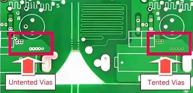
Tented vias are sealed with solder mask to prevent solder from wicking into the hole during SMT assembly, which can cause solder starvation on component pads. They also reduce long-term copper oxidation. However, poor mask application can lead to cracking or flux entrapment.
Untented vias leave the pad open, which is useful for thermal dissipation, test probing, or specific high-current applications, but they increase risks of solder defects and environmental corrosion.
The video provides clear guidelines: tent small vias near pads, keep most vias tented for protection, and intentionally leave vias untented only when thermal management or probing requires it. Proper via treatment is especially critical in high-reliability sectors such as aerospace, medical devices, and automotive electronics.
For projects requiring precise via specification, request an instant PCB quote. Explore advanced options with our HDI PCB capabilities or PCB assembly services where via tenting rules are strictly controlled.
KEY HIGHLIGHTS
- Tented vias prevent solder wicking during SMT assembly and protect copper from oxidation, improving manufacturing yield and long-term reliability.
- Untented vias are preferred for better heat dissipation or test probing but increase risk of solder defects and environmental exposure.
- Via tenting decisions must balance reliability, thermal management, and assembly process requirements - there is no one-size-fits-all solution.
Why Via Tenting Decisions Matter in Real Production
Via tenting is one of the most frequent items in Engineering Questions (EQs). Wrong choices lead to solder wicking, insufficient solder joints, or field failures from oxidation and contamination. Proper specification in your Gerber files and stack-up documentation prevents these issues before lamination and plating.
What Are Tented Vias vs Untented Vias?
- Tented Vias: Fully covered by solder mask on one or both sides. The mask overlaps the annular ring to seal the hole.
- Untented Vias: No solder mask coverage — copper pad and hole barrel remain exposed.
- Plugged or Filled Vias: A separate process where vias are filled with resin or conductive material (beyond simple tenting).
Key Differences and Manufacturing Impacts
| Aspect | Tented Vias | Untented Vias |
|---|---|---|
| Solder Wicking | Prevented | Higher risk during SMT |
| Oxidation / Corrosion | Excellent protection | Exposed to environment |
| Thermal Dissipation | Moderate | Better heat transfer |
| Test Probing | More difficult | Easy access |
| Assembly Yield | Generally higher | Requires tighter process control |
| Cost / Complexity | Standard process | May need additional masking steps |
DFM Best Practices for Via Tenting
- Tent all vias smaller than 0.3mm, especially near component pads.
- For thermal vias under pads, consider untented or filled/plugged.
- Specify tenting clearly in fabrication notes (e.g., "Tent all vias unless otherwise noted").
- Ensure minimum solder mask overlap (typically 0.05–0.1mm) on annular rings.
- In HDI designs, via tenting becomes even more critical due to smaller feature sizes.
Common Via-Related Failures and How to Avoid Them
From factory experience, poor tenting often causes:
- Solder starvation on fine-pitch pads.
- Mask cracking during reflow leading to flux entrapment.
- Long-term corrosion in humid or harsh environments.
Always review via treatment early in DFM to avoid costly respins.
FAQ
Q1: When should vias be tented versus left untented?
A1: Tent vias near component pads to prevent solder wicking and for most standard applications. Leave vias untented when you need enhanced thermal dissipation, easier probing, or specific high-current paths.
Q2: Do tented vias affect PCB reliability?
A2: Yes. Properly tented vias reduce oxidation risk and solder-related defects, significantly improving long-term reliability in harsh environments such as automotive, medical, and industrial applications.
Q3: How does via tenting impact SMT assembly?
A3: Tented vias prevent solder from flowing into the hole (solder wicking), avoiding insufficient solder on pads. Poor tenting, however, can trap flux or cause mask cracking during reflow.
Q4: What is the difference between tented vias and via plugging/filling?
A4: TTenting only covers the via with solder mask on the surface. Plugging or filling completely fills the hole with epoxy or conductive material for better planarity, thermal/electrical performance, or to meet IPC standards in high-reliability boards.
Q5: Should thermal vias under BGAs or QFNs be tented?
A5: Usually left untented or filled to maximize heat transfer to the copper plane. However, they must be properly masked on the opposite side to prevent solder wicking during assembly.
Ever seen tiny holes on a PCB — some covered, some left open — and wondered why that matters?
It's not decoration. It actually affects reliability.
Tented vias, are vias sealed with solder mask.
Untented vias expose the copper pad directly.
With untented vias, solder can accidentally wick into the hole — like water leaking through a drain — causing solder starvation on nearby pads.
Untented vias also expose copper to air, increasing oxidation risk over time.
But tented vias aren't perfect either — if the solder mask isn't applied well, it can crack or trap flux.
So what do engineers do?
Use tented vias near pads to prevent solder wicking.
Keep small vias tented to avoid oxidation.
Leave vias open when you need better thermal dissipation or easy probing.
There's no universal "best" choice — it depends on your layout and purpose.
This is aivon, making PCB learning easier, comment below — and follow for more PCB tips!





