Introduction
Vias serve as essential interconnects in printed circuit boards, enabling electrical continuity between different layers in multilayer designs. As PCB complexity increases with higher component densities and faster signal speeds, advanced via technologies become critical for maintaining signal integrity, reducing board size, and managing thermal performance. This article explores types of vias, key design rules, and optimization techniques tailored for electrical engineers working on high-density interconnects. Engineers must consider manufacturing constraints to ensure reliability, especially with blind via PCB structures, buried via PCB configurations, microvia design challenges, via in pad implementations, and thermal via placement strategies. Proper via selection directly impacts fabrication yield, assembly success, and long-term board performance. Understanding these elements aligns designs with industry expectations for robust multilayer boards.
Understanding Vias in PCB Manufacturing
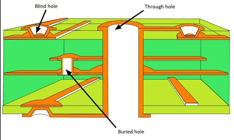
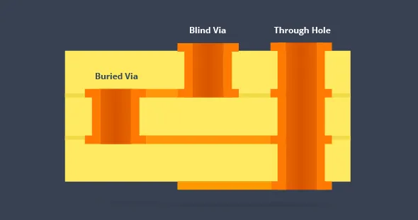
Vias are plated through-holes that provide vertical electrical connections across PCB layers, forming the backbone of multilayer interconnects. In standard through-hole vias, the hole extends from the top surface to the bottom, allowing plating to connect all layers but consuming significant board real estate. Blind vias start from one outer layer and terminate at an inner layer, saving space by not penetrating the full board thickness. Buried vias connect only inner layers, completely hidden from external surfaces, which optimizes routing density in complex stackups. These advanced vias require sequential lamination processes during manufacturing to achieve precise layer-to-layer connections. Factory insights reveal that via reliability hinges on plating uniformity and aspect ratio control to prevent voids or cracks under thermal stress.
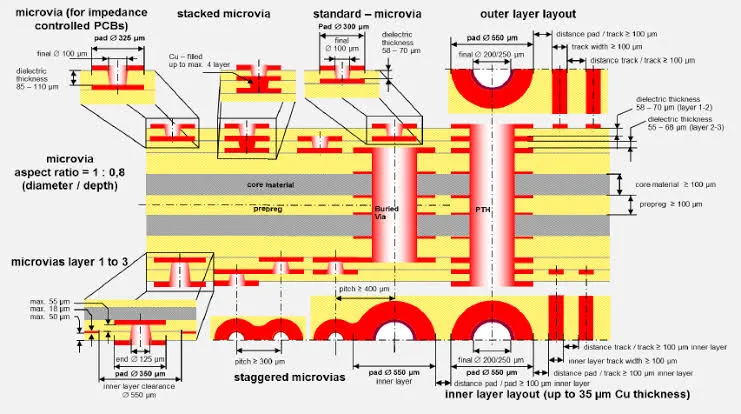
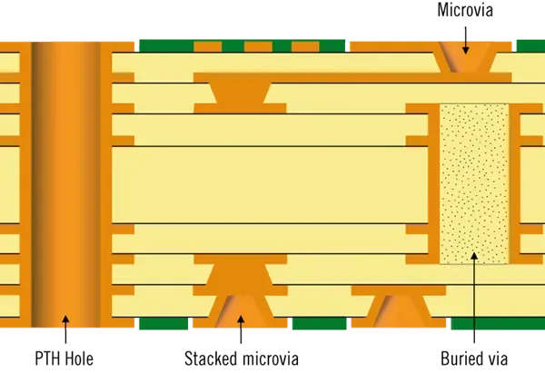
Microvias represent a subset of blind or buried vias with diameters typically under 150 micrometers, drilled using lasers for high precision in high-density interconnect boards. They enable finer pitch components and tighter routing, crucial for modern applications like smartphones and servers. However, microvia design demands careful stackup planning to avoid reliability issues such as cracking during reflow soldering. Manufacturers classify PCBs using these vias as HDI types, where via positioning influences overall board warpage and impedance control. Electrical engineers benefit from recognizing how via types balance density gains against fabrication costs and yield risks.
Types of Vias and Their Applications
Through vias offer simplicity and robustness, suitable for low-density boards where space is not constrained. They support high current carrying capacity due to larger diameters but increase parasitic inductance, affecting high-speed signals. Blind via PCB designs connect surface traces to one or more inner layers without reaching the opposite side, ideal for BGA fanout and reducing stub lengths for better signal integrity. These vias demand controlled depth drilling and plating to ensure connection quality. Buried via PCB configurations link inner layers exclusively, invisible on outer surfaces, which maximizes usable copper area on top and bottom layers for components and traces.
Microvias extend blind and buried capabilities to sub-150 micrometer scales, often filled with conductive or non-conductive materials for planarization. Stacked microvias align vertically across multiple layers, while staggered ones offset for better reliability. Via in pad places the via directly within a component pad, common in fine-pitch BGAs to shorten escape routes. Thermal vias, arrays of small plated holes under heat-generating components, transfer heat to inner planes efficiently. Each type suits specific density and performance needs, with factories prioritizing via types based on layer count and drill capabilities.
Key Design Rules for Reliable Via Implementation
Design rules for vias start with aspect ratio, defined as via depth divided by diameter, typically limited to 10:1 for through vias to ensure uniform plating per IPC-2221 guidelines. Blind and buried vias often target lower ratios like 0.8:1 to minimize plating voids, especially in thicker boards. Minimum via diameter depends on drill type, with mechanical drills at 0.15 mm and lasers enabling 0.075 mm for microvias. Annular ring width, the copper surround around the via, must meet minimums like 0.1 mm external and 0.075 mm internal to prevent breakout during fabrication. Pad diameter calculations follow IPC-2221 formulas, such as pad size equaling hole diameter plus twice the annular ring plus allowances for fabrication tolerances.
For microvia design, IPC-2226 specifies maximum aspect ratios of 1:1 and depth under 0.25 mm to maintain reliability in HDI stackups. Via in pad requires tenting or filling to prevent solder wicking during assembly, with non-conductive epoxy plugs ensuring planarity. Thermal via placement involves arrays of 0.3-0.4 mm vias spaced 0.5-1 mm apart under thermal pads, connected to power or ground planes for heat spreading. Engineers should simulate thermal resistance and verify drill-to-drill spacing to avoid shorting. These rules prevent common failures like via barrel cracks or delamination under cyclic thermal loads.
Optimization Techniques for Via Performance
Optimization begins with minimizing via count through intelligent routing, favoring wider traces over excessive interconnections where possible. For high-speed designs, back-drilling removes unused via stubs to reduce reflections, particularly effective for blind via PCB implementations. Filled vias enhance mechanical strength and thermal conductivity, using conductive paste for electrical continuity or epoxy for insulation in via in pad setups. Staggered microvias distribute stress better than stacked ones, improving fatigue resistance in flexing environments.
Thermal via placement optimization arrays vias in dog-bone patterns or grids, tented on the surface to block solder flow while open on inner layers for airflow cooling. Simulate via thermal impedance using finite element analysis to balance heat transfer against board thickness. Factory-driven techniques include sequential build-up for buried vias, controlling resin flow to encapsulate vias uniformly. Aspect ratio reduction via larger diameters trades density for reliability in critical applications. Compliance with IPC-6012 performance specs ensures plating thickness exceeds 20 micrometers in vias for corrosion resistance.
Best Practices and Manufacturing Considerations
Adopt a design-for-manufacturability approach by consulting fabricator DFM reports early, specifying via types and fills explicitly. Use copper-balanced stackups to minimize warpage from blind and buried vias, with symmetric layer pairing. For microvia design, limit stacking to two levels without via capture pads if reliability testing confirms. Thermal via placement should include stitching vias around the array periphery to enhance current spreading. Post-fabrication, inspect vias via cross-sectioning or electrical testing to verify continuity and plating quality.
Sequential lamination for advanced vias requires precise registration, with laser drilling post-outer layer lamination for blind structures. Avoid over-etching around vias to maintain annular ring integrity. In high-layer-count boards, buried via PCB techniques free outer layers for signals, improving EMI performance. Engineers gain from prototyping HDI panels to validate microvia yield before full production.
Conclusion
Via technology drives PCB evolution toward higher densities and performance, with blind via PCB, buried via PCB, microvia design, via in pad, and thermal via placement as cornerstones. Adhering to design rules like aspect ratios and annular rings ensures manufacturability and reliability. Optimization through filling, staggering, and simulation maximizes benefits while mitigating risks. Electrical engineers applying these principles achieve compact, robust boards aligned with industry standards. Future designs will leverage even finer vias, demanding ongoing expertise in HDI processes.
FAQs
Q1: What is a blind via PCB, and how does it differ from a through via?
A1: A blind via PCB features vias that connect an outer layer to one or more inner layers without penetrating the full board thickness, unlike through vias that span all layers. This design saves surface space and reduces signal stubs for better integrity. Manufacturing involves sequential drilling and plating, with aspect ratios under 1:1 recommended. Blind vias suit HDI for BGA escapes, but require precise depth control to avoid opens.
Q2: How does buried via PCB improve multilayer routing?
A2: Buried via PCB connects only inner layers, invisible externally, freeing top and bottom for components and traces. This boosts density in 8+ layer boards by enabling tighter inner routing. Factories use progressive lamination to form them, targeting low aspect ratios for plating uniformity. They complement blind vias in complex stackups, enhancing yield when diameters exceed 150 micrometers.
Q3: What are key considerations in microvia design for HDI PCBs?
A3: Microvia design limits diameters to 150 micrometers or less with 1:1 aspect ratios, often laser-drilled and filled. IPC-2226 guides stack types like 1+n+1 for reliability. Staggering prevents cracks, while filling ensures planarity for fine-pitch assembly. Engineers must balance density with thermal cycling tests to avoid failures.
Q4: What best practices apply to thermal via placement in power components?
A4: Thermal via placement uses arrays of 0.3 mm vias under thermal pads, spaced 0.6 mm, connected to inner planes. Tent surface ends to prevent solder wicking, and fill if via in pad. Optimize count via simulation for 20-50% heat reduction. This enhances dissipation without compromising electrical isolation.
References
IPC-2221 — Generic Standard on Printed Board Design. IPC.
IPC-6012E — Qualification and Performance Specification for Rigid Printed Boards. IPC, 2015.
IPC-2226 — Design Standard for High Density Interconnects. IPC.