










Flexible PCB Explained: Smart Choice for Modern Designs
Key Moment
What This Video Covers
This video explains how flexible PCBs (FPCs) enable compact, high-reliability electronics by bending and folding into tight spaces where rigid boards cannot fit. Built from thin polyimide substrates and copper layers, these circuits combine lightweight construction with exceptional mechanical endurance and repeated-flex reliability.
Polyimide's high-temperature resistance keeps assembly processes stable while maintaining signal integrity. The video highlights key manufacturing capabilities, including 1- to 8-layer FPC production, fine-line etching, laser drilling, and stiffener integration.
Engineers and procurement teams will see real-world applications in wearables, camera modules, automotive electronics, and other space-limited devices. For custom flexible PCB solutions, explore our flexible PCB capabilities and flexible PCB quote service. Automotive designers can also review our dedicated automotive PCB expertise.
Key Highlights
- Thin polyimide and copper construction delivers lightweight durability with repeated-bend reliability
- Excellent thermal stability supports stable assembly and high-temperature environments
- Ideal for space-constrained applications including wearables, automotive modules, and compact electronics
Polyimide Substrate Construction and Mechanical Performance
Flexible PCBs rely on polyimide film as the primary dielectric because the material retains mechanical strength and dielectric properties after thousands of flex cycles. Typical base thicknesses range from 12.5 µm to 50 µm; thinner films improve overall flexibility while thicker films increase tear resistance. Rolled-annealed (RA) copper is preferred over electrodeposited copper for dynamic-flex applications because its grain structure better accommodates repeated bending without cracking.
Coverlay films, usually polyimide with acrylic or epoxy adhesive, replace conventional solder mask in the flex zones. Coverlay openings are laser- or mechanically routed to expose pads while protecting traces from abrasion and moisture. When static flex or local reinforcement is required, polyimide, FR-4, or stainless-steel stiffeners are bonded with controlled-pressure lamination. Improper adhesive selection or excessive lamination temperature can introduce residual stress that later appears as delamination or trace fracture.
Layer Capabilities and Precision Manufacturing Processes
Production lines support single-sided, double-sided, and multilayer flexible circuits up to eight conductive layers. Fine-line etching routinely achieves 50 µm line/space on outer layers and 75 µm on inner layers when using adhesiveless polyimide laminates. Laser drilling creates micro-vias as small as 50–75 µm diameter, enabling high-density interconnects without the mechanical stress of mechanical drilling.
Panelization, coverlay registration, and surface-finish plating (ENIG, ENEPIG, or immersion silver) are performed under controlled humidity and temperature to limit dimensional change. Each lot undergoes 100 % electrical testing plus sample flex-life testing that cycles the circuit through a defined bend radius for a specified number of cycles. These process controls reduce the risk of latent opens or intermittent shorts that only appear after field installation.
Application Suitability in Wearables, Automotive, and Compact Modules
In wearable devices, flexible PCBs conform to curved surfaces and survive continuous motion without bulk. Camera modules and foldable displays rely on the same thin, high-density construction to route signals through hinge regions. Automotive applications exploit the vibration damping and thermal endurance of polyimide to place circuits near engines, sensors, and battery packs where rigid boards would require additional connectors and occupy excess volume.

When the same design must operate across –40 °C to +125 °C or higher, the coefficient-of-thermal-expansion match between polyimide and copper becomes critical. Mismatch can generate cyclic stress that accelerates copper fatigue; proper stack-up design and controlled copper weight mitigate this risk.
Critical DFM Rules That Determine Flexible PCB Reliability
Bend radius is the single most important geometric rule. For dynamic flex, a minimum bend radius of 10× finished thickness is typically required; static flex can accept 6×. Traces in the bend area must run perpendicular to the bend axis and should be staggered rather than stacked directly above one another. Solid copper pours are avoided in flex zones; hatched pours or reduced copper weight lower stiffness.
Vias and plated through-holes are kept outside the dynamic bend region. When vias are unavoidable, teardrop pads and non-conductive fill reduce stress concentration. Coverlay openings are oversized relative to pads by at least 0.1 mm per side to accommodate registration tolerance. Stiffener edges are placed at least 0.5 mm away from the start of the bend zone to prevent abrupt stiffness transitions that initiate cracks.
Designers who ignore these rules commonly encounter copper cracking after a few hundred cycles or adhesive separation at the stiffener interface. Early DFM review that includes bend-radius simulation and stack-up analysis prevents most of these failures before tooling is committed.
| Parameter | Typical Capability | DFM Recommendation |
|---|---|---|
| Layer count | 1–8 | Keep dynamic flex zones ≤ 2 layers |
| Minimum line/space | 50 µm / 50 µm (outer) | Increase to 75 µm in high-flex areas |
| Minimum bend radius (dyn.) | 10× thickness | Verify with actual stack-up thickness |
| Copper type | RA preferred for dynamic | ED acceptable only for static flex |
| Coverlay thickness | 12.5–25 µm | Match adhesive flow to copper thickness |
| Stiffener materials | PI, FR-4, stainless steel | Locate edges outside bend region |
Common Production Failure Modes and Prevention Measures
Copper fracture in the bend zone remains the most frequent field failure. It originates from excessive local strain, sharp radius transitions, or the use of electrodeposited copper in dynamic applications. Delamination between coverlay and copper occurs when moisture is trapped during lamination or when surface preparation is incomplete. Via barrel cracks appear when micro-vias are placed inside the flex region and experience repeated tensile stress.
Prevention begins with material selection (adhesiveless polyimide + RA copper), continues through controlled lamination parameters, and ends with lot-level flex testing that replicates the customer’s bend radius and cycle count. In-process optical inspection after etching and after coverlay application catches registration and coverage defects before final plating. When these controls are applied consistently, first-pass yield for complex multilayer FPCs routinely exceeds 95 %.
FAQ
Q1: How many layers can flexible PCBs reliably support in production?
A1: Our capabilities cover 1- to 8-layer FPC with fine-line etching and laser drilling for complex designs.
Q2: What design factors most affect flexible PCB reliability during repeated bending?
A2: Bend radius, material stack-up, and stiffener placement directly impact long-term mechanical endurance and signal performance.
Q3: Are flexible PCBs suitable for automotive electronics applications?
A3: Yes—polyimide-based FPCs offer vibration resistance, thermal stability, and space-saving routing ideal for automotive control modules and sensors.
Q4: What is the recommended minimum bend radius for a dynamic-flex flexible PCB?
A4: Industry practice sets the dynamic minimum bend radius at approximately 10 times the finished circuit thickness. Static-flex applications may accept 6 times thickness, provided the copper is oriented correctly and no vias lie in the bend zone.
Q5: How do stiffeners affect assembly and long-term reliability?
A5: Stiffeners locally increase rigidity under connectors or components, protecting solder joints from flex-induced stress. Edges must be located outside the intended bend region; abrupt transitions create stress risers that initiate cracks. Material choice (polyimide, FR-4, or metal) is matched to the required stiffness and thermal-expansion needs.
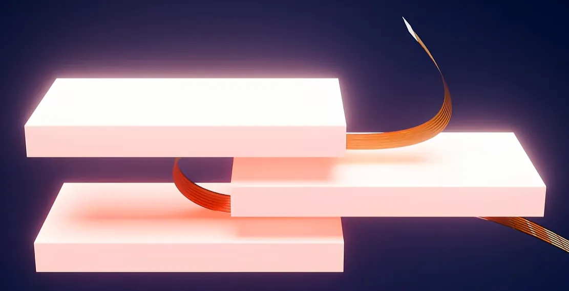
This is a Flexible PCB — a circuit that can bend, fold, and adapt to tight spaces.
Built from thin polyimide and copper layers, it stays light while offering strong mechanical endurance.
Its biggest advantage is reliability: it maintains performance even after repeated bending.
It also frees up space, enabling routing where rigid boards can't reach.
And polyimide handles high temperatures well, so assembly stays stable.
You'll find flexible PCBs in wearables, camera modules, automotive parts, and pretty much any device where space is limited.
We support 1 to 8-layer FPC, fine-line etching, laser drilling, and stiff ener assembly.
If your design needs flexibility — literally — FPC is often the smartest choice.
Get your quote now and discover smarter PCB manufacturing — start your project and explore processes with Aivon.





