










Rigid-Flex PCB: Strength and Flexibility in One Hybrid Design
Key Moment
What This Video Covers
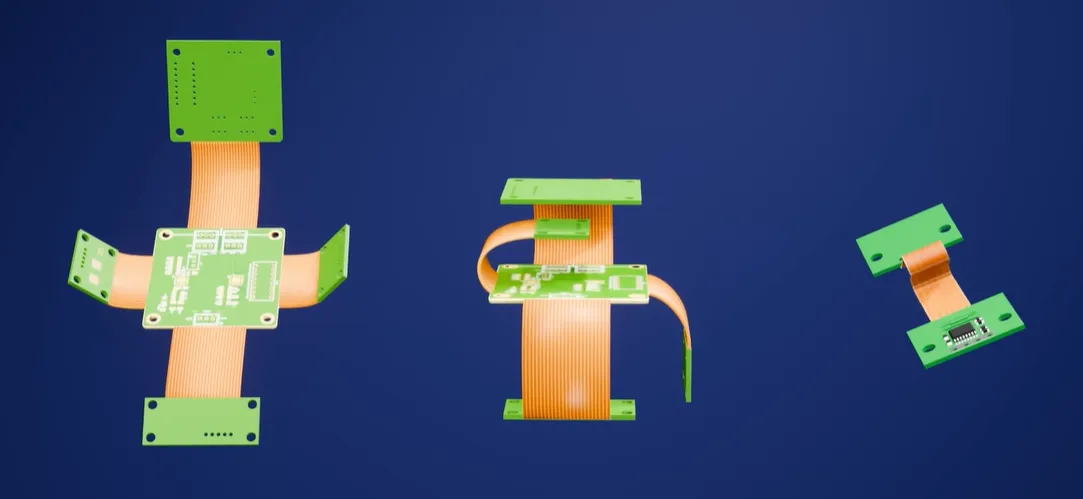
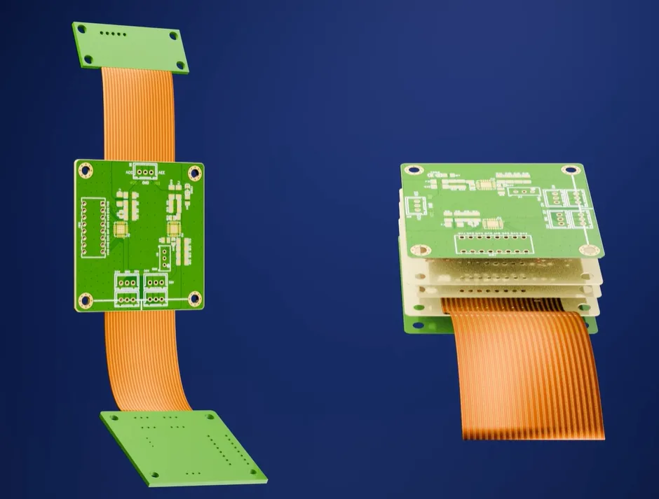
This video explains how Rigid-Flex PCBs integrate the mechanical strength of multilayer FR4 with the adaptability of polyimide sections in a single board. The hybrid construction allows signals to flow seamlessly between rigid and flexible areas, eliminating connectors and improving long-term reliability.
Designers gain significant space savings and layout freedom for compact electronics while maintaining excellent thermal endurance during assembly and operation. Key manufacturing capabilities highlighted include multi-layer Rigid-Flex builds, controlled impedance routing, laser drilling, and selective stiffener reinforcement.
Real-world applications span smartphones, medical devices, aerospace systems, and other high-performance environments where both strength and flexibility are essential. For detailed specifications, explore our rigid-flex PCB capabilities. Engineers can also request a custom quote through our dedicated rigid-flex PCB quote service, or review application-specific guidance in our aerospace PCB resources.
Key Highlights
- Hybrid multilayer FR4 and polyimide construction delivers mechanical stability plus design flexibility
- Controlled impedance routing and laser drilling enable seamless signal flow while reducing connectors
- Proven performance in space-critical applications including smartphones, medical devices, and aerospace systems
Critical Manufacturing Processes for High-Reliability Rigid-Flex PCBs
Multi-layer lamination of dissimilar materials (FR4 and polyimide) requires precise control of temperature, pressure, and dwell time to manage coefficient-of-thermal-expansion (CTE) mismatch. Inadequate process parameters commonly produce delamination at the rigid-to-flex interface, residual stress, or dimensional instability that appears only after thermal shock or reflow.
Controlled impedance routing must account for the lower dielectric constant of polyimide relative to FR4. Impedance test coupons representing the actual flex-zone stack-up (including coverlay) are required; standard rigid-board calculations produce unacceptable variation. Laser drilling supports high-density microvias but demands tight aspect-ratio limits and thorough desmear to ensure reliable plating in blind structures.
Selective stiffener reinforcement (FR4 or polyimide) is applied only under component or connector areas. Incorrect adhesive thickness or placement tolerance leads to pad coverage, uneven support, or stress concentration at the stiffener edge during flexure.
Transition Zone Design and Stress Management Challenges
The rigid-to-flex transition is the most frequent location of field failures in Rigid-Flex PCBs. Copper traces experience cyclic strain when the flex section bends; without adequate bend radius (typically ≥10× flex thickness for static applications) and smooth geometric transitions, fatigue cracking initiates at the copper–dielectric interface.
Sharp corners, abrupt copper width changes, or vias placed inside or immediately adjacent to the bend region concentrate stress and accelerate crack propagation. Balanced copper distribution on opposing layers and the use of rolled-annealed copper in dynamic or high-cycle zones reduce residual stress. Coverlay openings and adhesive fillets must be designed to avoid abrupt thickness steps that create stress risers.
In production, controlled-depth routing defines the transition edge. Insufficient depth control leaves residual rigid material that restricts flexure or exposes copper that later corrodes. Early DFM review of transition geometry, via keep-out zones, and copper balance prevents these progressive failure modes before tooling is committed.
Stiffener Selection, Placement, and Common Failure Modes
Stiffeners provide local rigidity under connectors, BGAs, or soldered components while allowing the remaining flex section to bend. FR4 stiffeners are preferred for component support; thinner polyimide stiffeners are used where weight or profile must be minimized.
Placement clearance must exceed the combined manufacturing tolerances of stiffener cutting, adhesive application, and registration (typically >0.25 mm per side). Insufficient clearance results in stiffener overlap of pads or vias, blocking soldering or creating open circuits. Stiffeners located too close to the intended bend line force a sharp crease at the stiffener edge, rapidly initiating copper fatigue.
Adhesive thickness and uniformity are critical. Excess adhesive can flow into vias or create air pockets that expand during reflow, producing delamination. Incomplete adhesive coverage allows the stiffener to shift under mechanical load. Production practice requires verification of stiffener outline against finished board dimensions and confirmation that mechanical support holes include additional tolerance for later assembly alignment.
Practical Comparison of Rigid, Flex, and Rigid-Flex Approaches
| Parameter | Traditional Rigid PCB | Pure Flex PCB | Rigid-Flex PCB |
|---|---|---|---|
| Mechanical support | High | Low (requires stiffeners) | High in rigid zones |
| Connector count | High | Moderate | Minimal (integrated interconnect) |
| Space / 3-D packaging | Limited | Excellent | Excellent |
| Vibration / shock reliability | Moderate | Good | Highest (no discrete connectors) |
| Typical layer range | 2–20+ | 1–6 | 4–20+ |
| Primary failure risk | Connector contacts | Copper fatigue in bend | Transition-zone delamination or stress |
| Best application fit | Standard assemblies | Dynamic flexing | Compact, high-reliability systems |
FAQ
Q1: How does a Rigid-Flex PCB reduce connector count compared to separate rigid and flex boards?
A1: By integrating rigid and flexible sections into one board, signals flow seamlessly without additional connectors, improving reliability and assembly simplicity.
Q2: What manufacturing processes are most critical for high-reliability Rigid-Flex designs?
A2: Multi-layer lamination, controlled impedance routing, laser drilling, and selective stiffener reinforcement ensure mechanical endurance and signal integrity.
Q3: Are Rigid-Flex PCBs suitable for aerospace and medical device applications?
A3: Yes—polyimide and FR4 hybrids provide vibration resistance, thermal stability, and compact layouts required for avionics, medical implants, and portable diagnostic equipment.
Q4: What is the recommended minimum bend radius for a Rigid-Flex PCB flex section?
A4: For static (one-time or infrequent) bends, a minimum radius of 10× the total flex thickness is standard practice. Dynamic or repeated flexing generally requires larger radii and is often better addressed with pure flex constructions. Insufficient radius concentrates strain and initiates copper fatigue cracks at the transition zone.
Q5: Why do Rigid-Flex PCBs sometimes delaminate after reflow or thermal cycling?
A5: CTE mismatch between FR4 and polyimide, combined with residual stress from unbalanced copper or inadequate lamination parameters, creates interfacial forces that exceed bond strength. Symmetric stack-ups, proper no-flow prepreg selection, and controlled cooling rates after lamination significantly reduce this risk.
This is a Rigid-Flex PCB — a hybrid circuit that combines the strength of rigid boards with the adaptability of flexible ones.
Built from multilayer FR4 and polyimide, it delivers both mechanical stability and design freedom.
Its biggest advantage is integration: signals can flow seamlessly across rigid and flexible sections, reducing connectors and improving reliability.
It also saves space, enabling compact layouts where traditional rigid boards would be too bulky.
And with excellent thermal endurance, assembly remains stable even under demanding conditions.
You'll find Rigid-Flex PCBs in smartphones, medical devices, aerospace systems, and any application where performance and space optimization are critical.
If your design needs both flexibility and strength — Rigid-Flex PCB is often the smartest choice.
We support Multi-layer Rigid-Flex designs, controlled impedance routing, laser drilling, and selective stiffener reinforcement.
Get your quote now and discover smarter PCB manufacturing — start your project and explore processes with Aivon.





