










-
 02:50
02:50
Via Treatment Issues Video: Why Manufacturers Ask About Via Openings
Via treatment is a small PCB specification that can create major manufacturing issues when its intended finish is unclear. This video shows how choices such as tenting, opening, plugging, and resin filling affect solder mask coverage, drilling, plating, and the final behavior of vias on FR4 and HDI boards. It also explains why a design can pass normal DRC checks yet still require clarification when fabrication data, notes, and ordering information point to different via finishes. Special attention is given to via-in-pad designs, large plated holes, and boards that use more than one via treatment, where inconsistent documentation can lead to unexpected mask openings, solder wicking, or assembly defects. A clear manufacturing package should define the required via finish and keep every production file aligned before PCB prototyping, mass production, or PCBA assembly begins.
-
 03:41
03:41
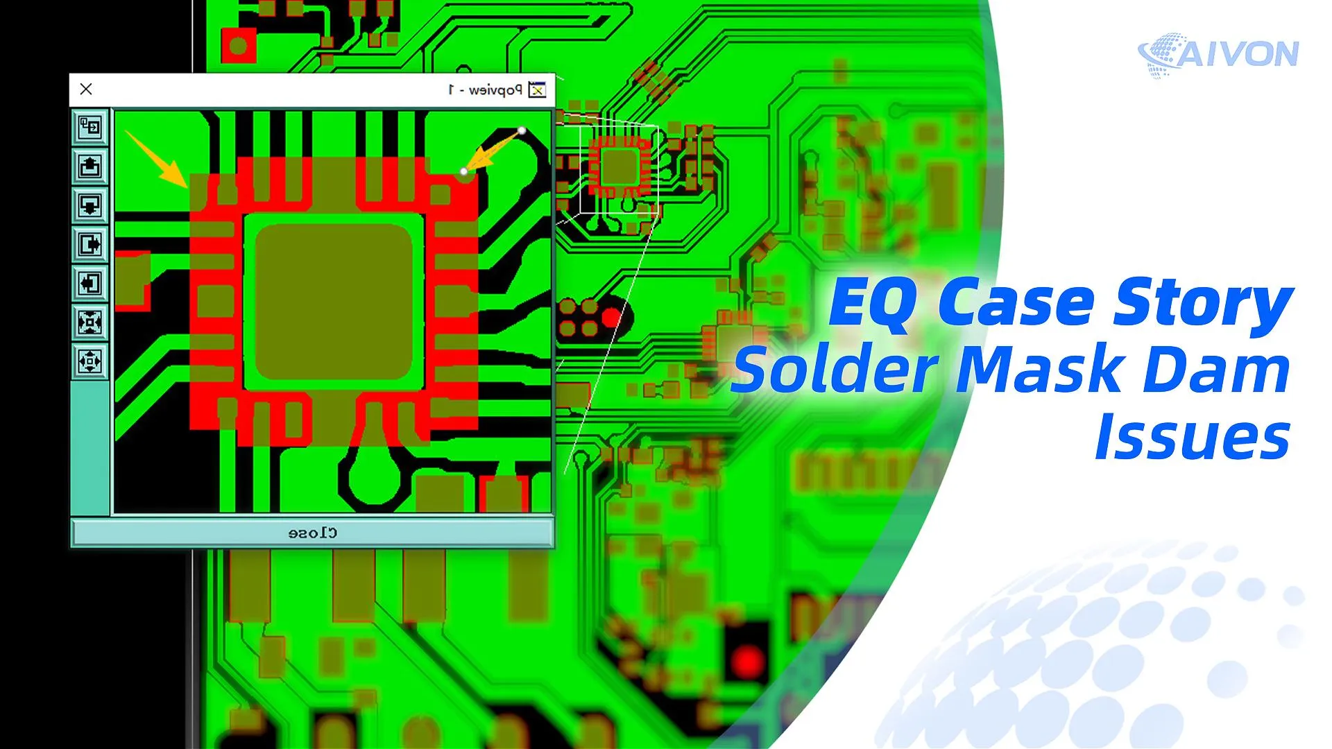
PCB Solder Mask Bridges Issues: Fine-Pitch DFM
This engineering-review video explains why CAM teams check solder mask bridges even when copper DRC shows no errors. Because solder mask openings are typically expanded beyond the copper pads, narrow gaps can leave a mask dam that is too thin to print reliably and may flake, merge, or disappear during production. The video examines practical cases involving fine-pitch SMT pads, NSMD and SMD BGA pads, different solder mask colors, and copper weights, as well as situations where a solder mask dam should be restored or removed, such as unnecessary gang openings and gold-finger areas. These considerations are important for HDI PCB layouts, 4-layer and 6-layer PCB prototypes, and high-density QFP, QFN, BGA, and connector assembly. Review solder mask layers and pad spacing before requesting a PCB quote or PCBA quote, then let CAM confirm the final design against actual mask, color, and copper process capabilities.
-
 05:29
05:29
PCB Silkscreen Issues: Put Orders on Hold Even After DRC Passes
This video examines four real-world PCB production holds caused by silkscreen issues that passed electrical DRC but failed manufacturing checks. It explains why silkscreen is more than on-screen geometry, as physical printing is affected by registration tolerance, print resolution, surface topography, and solderability requirements. The cases cover silkscreen overlapping exposed pads, text below minimum printability limits, conflicting or unclear markings across Gerber layers, and markings interacting with dense copper or BGA areas. These examples demonstrate why early DFM review of silkscreen clearance, text size, layer definition, and surface interaction is essential for reliable PCB assembly and production release.


