In early 2026, we received an order for a complex 18-layer PCB measuring 235.55 × 187 mm with 2.0 mm finished thickness. This board featured TG170 FR-4 material, ENIG surface finish, impedance control, resin-plugged vias, and selective back drilling. While the design intent was clear for a high-reliability application, the CAM engineering review revealed several manufacturability gaps that required immediate clarification to avoid production risks.
Multi-layer impedance-controlled boards with mixed via structures are among the most challenging for fabrication. Small deviations in material properties, copper distribution, or via processing can lead to serious yield loss. Our CAM team identified multiple issues during data preparation that highlight why thorough DFM review is essential before releasing files to production.
Order Overview
This was a 18-layer rigid PCB ( #FR4-20260327-031 ) built on FR-4 TG170 material with 0.5 oz copper on inner and outer layers. Finished board thickness was specified at 2.0 mm, with minimum hole size of 0.2 mm. The design included four-line low resistance testing, ENIG surface finish, and selective via resin plugging. Panelization was 1×2 with customer self-panelization, and the order quantity was 10 pcs (5 sets). Impedance control was required, and the stackup involved careful dielectric matching for signal integrity.
Special processes included back drilling on specific vias (noted around positions 18-15 and similar locations), mechanical forming, and addition of serialization, logos, and QR codes. The combination of high layer count, tight tolerances, resin plugging in BGA areas, and back drilling made this a classic case where design data needed alignment with actual manufacturing capabilities.
Critical DFM Issues Found in 18-Layer PCB CAM Engineering Review
1. Material Substitution and Impedance Stackup Adjustment
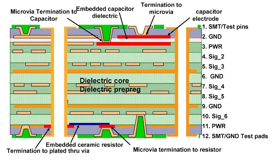
The original fabrication notes referenced M6 material. After internal review, our material engineering team recommended switching to our high-speed equivalent R5775G to better match current inventory and impedance performance requirements. We prepared a detailed stackup and impedance line adjustment proposal based on the customer’s impedance specifications and available dielectric materials.
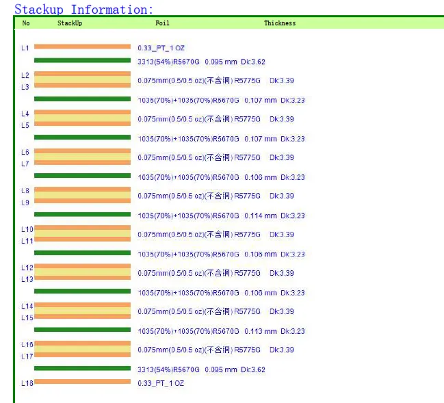
Figure 1: R5775G Material Parameters
We noticed that direct use of the original material parameters would have resulted in impedance values falling outside the target tolerance range due to differences in Dk and resin content. After reviewing the stackup, we adjusted the press parameters and line widths accordingly and sent the comparison file for confirmation.
If this adjustment had been ignored and production proceeded with mismatched material, the board could have exhibited signal integrity problems, including reflections and timing issues, potentially causing complete functional failure in the end product. According to typical IPC-2221 guidelines for controlled impedance, such mismatches often lead to scrap rates exceeding 30% in high-layer boards.
| Aspect | Original (M6) | Recommended (R5775G) | Benefit |
|---|---|---|---|
| Impedance Match | Out of tolerance | Within target | Better signal integrity |
| Availability | Limited | In-stock equivalent | Reduced lead time |
| Adjustment Needed | None | Line width & press params | Higher yield |
2. Large Copper-Free Areas on Inner Layers – Lamination Risk
Our CAM engineer identified one inner layer with a large continuous area completely devoid of copper. During lamination of 18-layer boards, unbalanced copper distribution creates significant stress. In 18-layer builds, such large voids disrupt uniform resin flow under high pressure, amplifying risks especially with TG170 material's thermal properties.
Figure 2: A large continuous area completely devoid of copper.
To mitigate this, we suggested adding production copper pour with 1.0 mm filleting at corners for better resin flow and stress relief. We asked the customer to confirm whether this modification was acceptable, as it would not impact electrical performance but would significantly improve manufacturing yield.
Had this issue gone unaddressed, the panel could have suffered severe warpage or delamination during pressing, leading to total scrap of the 18-layer stack. We have seen similar cases where unbalanced copper distribution caused resin voids and inner layer shorts after etching.
3. Back Drilling Confirmation for Multiple Vias in High-Layer PCB
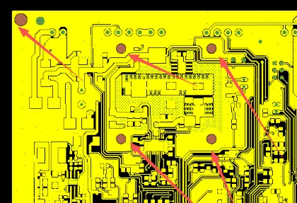
The design specified back drilling on via 18-15. However, our review found eight additional similar via locations with comparable depth and stub requirements. We needed confirmation whether these should also receive back drilling to maintain consistent signal integrity across the board.
Figure 3: Eight additional similar via locations
Original data showed inconsistency in back drill definitions between two reference positions, which we corrected in the production files after customer clarification. Our engineer noted that inconsistent back drilling would create varying stub lengths, directly impacting high-speed signal performance.
If left unconfirmed, some vias might have retained excessive stubs, leading to resonance issues, while others could have been over-drilled, risking via cracking or plating damage. In high-layer count boards, uncontrolled stubs are a common cause of signal instability.
4. Resin Plugged Vias and Solder Mask Opening Conflicts in BGA Area
The order required via resin plugging, but several plugged vias had solder mask openings larger than the hole diameter yet smaller than the pad. This configuration risked solder mask ink flowing onto the pad surface. In the BGA region, such openings could seriously affect solder paste deposition and joint reliability.
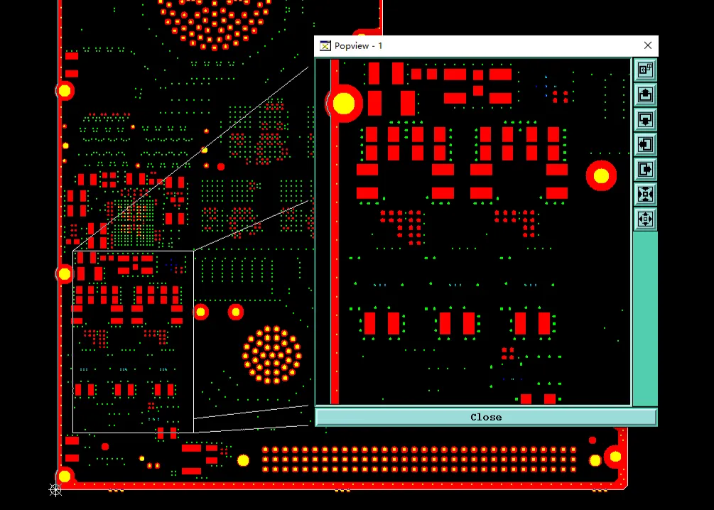
Figure 4: Several plugged vias had solder mask openings larger than the hole diameter
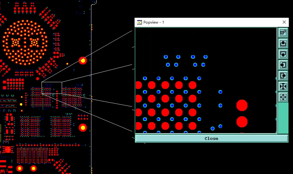
Figure 5: Several plugged vias had solder mask openings smaller than the pad
Our CAM team flagged this immediately because double-sided partial openings combined with resin plugging often lead to cosmetic and functional defects. We requested customer confirmation on the intended mask design for these vias.
Ignoring this would likely cause solder mask encroachment on pads, resulting in poor solderability, open joints, or BGA assembly failures. In extreme cases, resin plug voids combined with mask misalignment could lead to via cracking under thermal stress during assembly or field operation.
5. Serialization, Logo, and QR Code Requirements
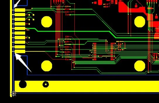
The customer requested addition of serial numbers, logos, production cycle codes, and QR codes. However, the QR code content was not specified, and initial data showed positioning issues (e.g., missing serial number at J9 location). We clarified the exact content and updated positions in the production files.
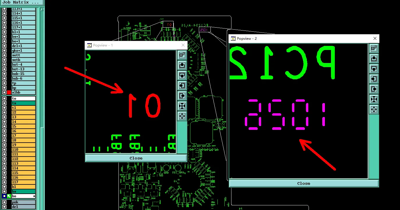
Figure 6: QR code content was not specified
Such marking details, while seemingly minor, are critical for traceability in production and quality control.
Manufacturing Risks and DFM Insights for High-Layer Impedance PCB
This case perfectly illustrates common pitfalls in high-layer impedance designs. Unbalanced copper distribution is one of the top triggers for lamination failures in 16+ layer boards. Designers often focus on signal routing and forget the mechanical implications of copper density during pressing.
Back drilling specifications are another frequent source of EQs. Without clear layer-by-layer definitions, CAM engineers must guess intent, which risks either insufficient stub removal or unnecessary drilling that weakens the board.
Via treatment in BGA areas with resin plugging requires extremely precise coordination between drill files, mask layers, and plugging parameters. Mismatches here commonly cause assembly yield drops of 10-20% if not caught early.
| Issue | Root Cause | Potential Impact | Resolution |
|---|---|---|---|
| Copper-Free Areas | Unbalanced distribution | Delamination/warpage | Add production pour |
| Back Drilling | Inconsistent locations | Signal resonance | Standardized via list |
| Plugged Via Mask | Opening size mismatch | Solderability issues | Precise pad/hole coordination |
How the Engineering Team Resolved the Issues
Our engineering team worked closely with the customer through multiple rounds of clarification. We provided annotated screenshots, revised stackup files, and production-ready Gerber/ODB packages for each change. The material switch to R5775G was approved with adjusted impedance lines. Copper balancing was implemented after confirmation. Back drilling locations were standardized, and mask via openings were corrected to prevent ink encroachment.
To reduce manufacturing risk, our CAM engineer adjusted the production data for consistent panelization copper and filleting while preserving all functional copper features. All serialization elements were properly positioned and verified.
Final Manufacturing Outcome
After receiving customer approvals on all engineering questions, the production data was finalized and released to the factory. The board successfully passed internal DFM checks and moved into the production queue with optimized parameters for lamination, drilling, and plating. Engineering clarification was completed without major redesign, protecting both schedule and quality.
Key Takeaways for High-Layer PCB Designers
- Always provide complete material specifications and allow manufacturer-recommended equivalents when possible for better impedance matching and availability.
- Balance copper distribution across all layers, especially in high-layer count boards. Large copper-free zones should be flagged and discussed early.
- Clearly define back drill requirements with specific via lists or layer pairs. Inconsistent stub control is a major signal integrity risk.
- For resin-plugged vias in BGA regions, coordinate solder mask openings carefully to avoid pad contamination or assembly issues.
- Include precise marking requirements (content, position, font) in fabrication notes to prevent last-minute revisions.
- Submit full impedance requirements with target values, tolerances, and reference layers early in the quoting stage.
- Use consistent layer naming and provide readable fabrication drawings that match the digital data.
FAQ
Q1: Why is copper balancing important in multi-layer PCB lamination?
A1: Unbalanced copper distribution creates uneven pressure and thermal expansion during lamination, leading to warpage, delamination, or board explosion. Adding production copper in void areas significantly improves yield for 16+ layer boards.
Q2: What happens if back drilling is not clearly specified?
A2: Vias may retain excessive stubs causing signal resonance or be over-drilled causing reliability issues. Consistent definition across similar vias is critical for high-speed designs.
Q3: Can resin-plugged vias have solder mask openings?
A3: Yes, but the opening size must be carefully controlled. Openings larger than the hole but smaller than the pad often cause mask ink to cover pads or create voids, affecting BGA soldering reliability.
Q4: Why do factories sometimes suggest material changes for impedance-controlled boards?
A4: Different materials have varying Dk values and resin contents. Using in-stock high-performance equivalents often achieves better impedance tolerance and avoids long lead times while maintaining design performance.
Q5: What is the risk of large copper-free areas on inner layers?
A5: Resin flow becomes uneven, causing wrinkles, voids, or delamination. In severe cases, the entire panel can be scrapped due to lamination failure.
Q6: How important is precise marking information in fabrication data?
A6: Extremely important for traceability. Incomplete QR code content or wrong positioning leads to repeated data revisions and potential quality tracking issues downstream.