Introduction
This case involves a 2-layer, extra-thick 3.0mm FR-4 PCB measuring approximately 406.4 × 660.4 mm. Designed for a rugged application with multiple countersunk holes, the order presented several manufacturability challenges during our standard CAM engineering review.
Thick boards with countersunk features are prone to mechanical and process-related issues. Large panel sizes further amplify risks around dimensional stability, copper distribution, and mechanical processing. Our CAM team identified inconsistencies between the provided fabrication notes, Gerber data, and actual manufacturing capabilities that required multiple rounds of clarification with the customer.
This engineering review case demonstrates why thorough DFM analysis before production is essential, particularly for thick, mechanically demanding PCBs. Ignoring these details could have led to dimensional inaccuracies, plating defects, or cosmetic failures after assembly.
Order Overview
The project was a 2-layer FR-4 board with TG150 material, 1oz copper on both sides, and a finished board thickness of 3.0mm (#FR4-20260425-090). Surface finish specified as immersion gold. Minimum hole size was 0.4mm with 100% flying probe testing required. The order quantity was 5 single pieces (1x1 panelization), with mechanical profiling and no V-cut. Delivery was set at 14 days.
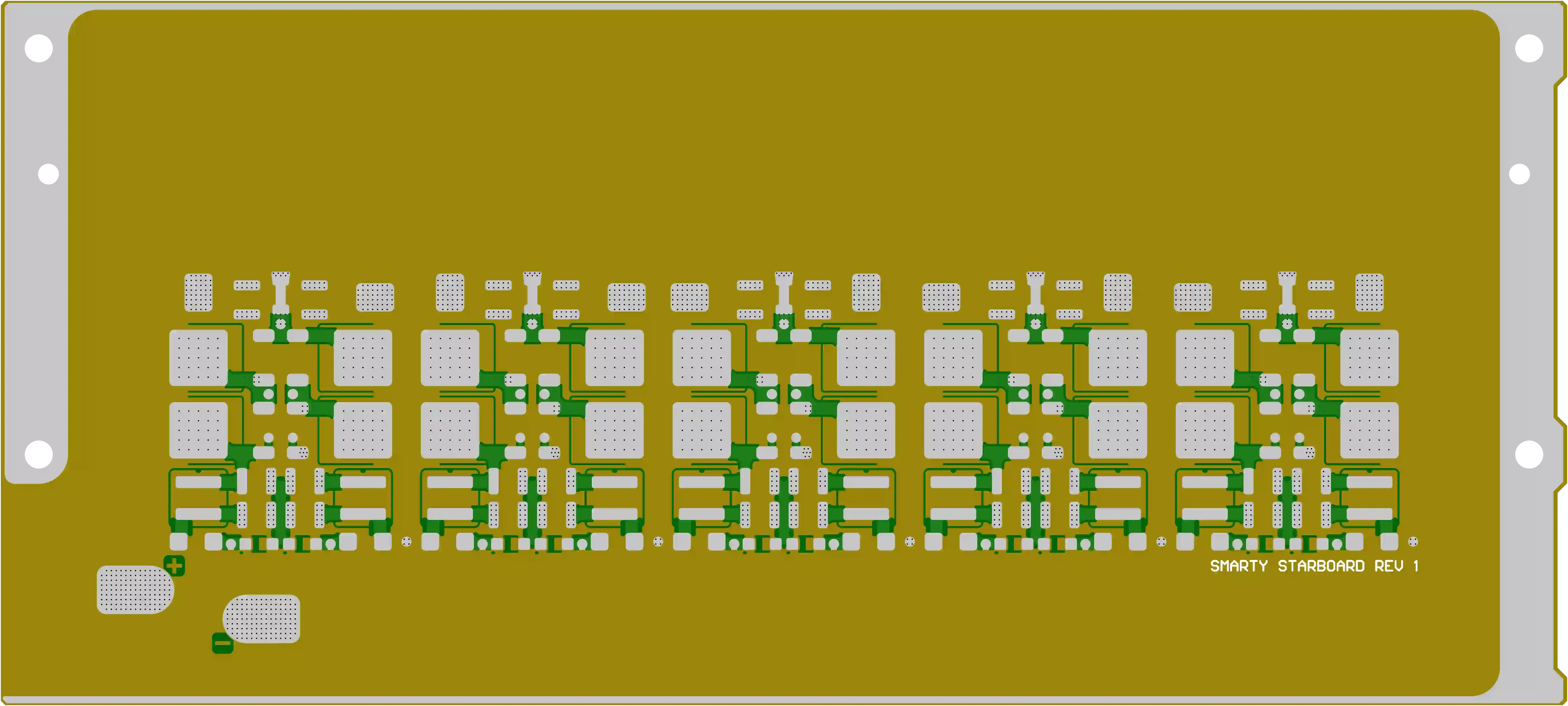
Key mechanical features included multiple countersunk holes and custom markings including a QR code and copyright text. While the base stackup looked straightforward, the combination of thick core material, precise countersink requirements, and conflicting documentation triggered a detailed engineering review.
Main Engineering Questions Found During CAM Review
1. Countersunk Hole Dimension & Tooling Angle Mismatch
Our engineer noticed a clear discrepancy between the customer's fabrication notes and the actual drill data. The notes specified 8.63mm diameter countersunk holes at an 82° angle, yet the provided data contained 7.87mm holes. Additionally, we do not stock the exact 82° tool and could only source an 8.6mm 90° countersink tool.
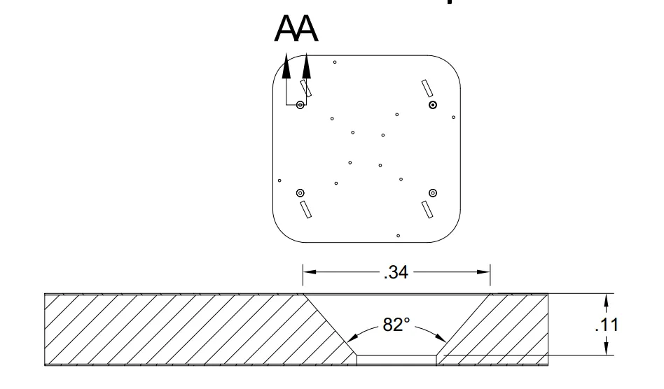
Figure 1: Specified 8.63mm diameter countersunk holes at an 82° angle
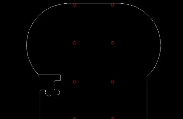
Figure 2: designed countersunk hole CAM diagram
We raised this as a priority EQ and asked for confirmation on tool replacement and which dimension set to follow. After internal discussion, we also needed clarification on sinking direction (TGL to GBL side) and reference documentation.
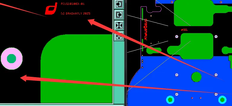
Figure 3: Sinking direction (TGL to GBL side)
If ignored, using mismatched tooling could result in incorrect countersink depth and angle, leading to poor screw seating, mechanical stress during assembly, or even board cracking around the holes. In thick 3.0mm material, improper countersinking significantly increases the risk of delamination or resin cracking due to uneven pressure distribution.
2. Finished Copper Thickness Specification (0.5oz Requirement)
The customer's attachment requested 0.5oz copper, but the base order parameters and supplied material indicated standard 1oz starting copper. We confirmed we did not have suitable 0.5oz core material in stock for this thick 3.0mm build.
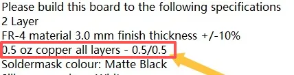
Figure 4: The customer's attachment requested 0.5oz copper
“After reviewing the stackup and fabrication notes,” our senior CAM engineer noted, “we recommended confirming the target finished copper weight because starting with thinner foil on a 3mm core would affect etch uniformity and mechanical strength.”
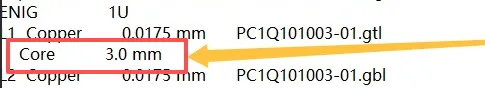
Figure 5: Requested 3mm core
Proceeding without clarification could have caused over-etching, trace width reduction below tolerance, or insufficient copper for current-carrying requirements, potentially leading to open circuits or thermal issues in the final product.
3. D-Shaped Holes & Copper Clearance on Outline
The outer profile included four D-shaped holes that did not maintain adequate copper clearance. Our CAM team identified this as a high-risk area for edge breakout or exposed copper after routing.
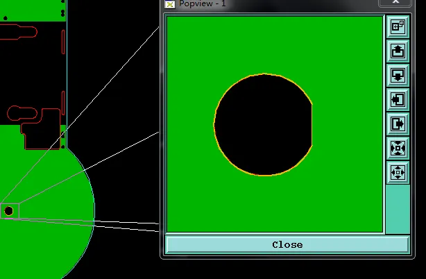
Figure 6: Four D-shaped holes that did not maintain adequate copper clearance
We suggested adjusting the copper pour or adding relief to prevent copper exposure on the mechanical edge. If left unaddressed, post-routing copper slivers or exposed traces near the board edge could cause short circuits during handling or assembly, especially problematic on a large board with immersion gold finish where edge quality is critical for reliability.
4. QR Code, Copyright Marking & Silkscreen Conflicts
Multiple questions arose regarding the QR code position, orientation, and content. The customer requested a second line with “(C)DRAGANFLY 2025” in the marking area, but existing top-layer silkscreen already occupied the space. Additionally, printing white QR code on a white solder mask block would result in poor readability.
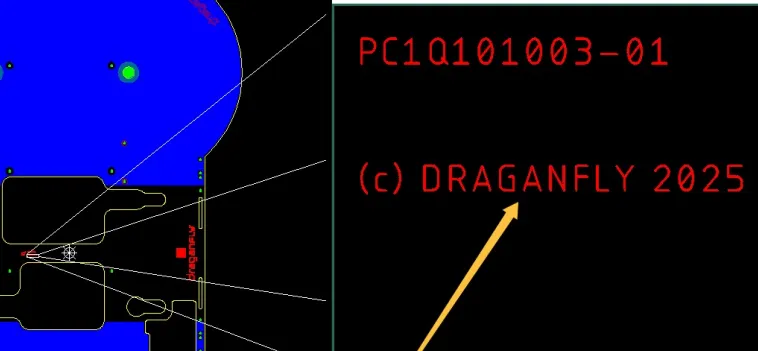
Figure 7: Requested second line with “(C)DRAGANFLY 2025” in the marking area
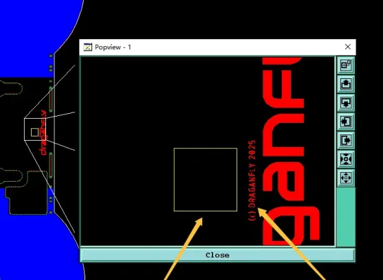
Figure 8: White QR code on a white solder mask block
We also confirmed whether the year should be updated to 2026. These seemingly minor cosmetic issues can cause production delays if not resolved early, as silkscreen and legend data must be finalized before photo plotting.
Manufacturing Risks and DFM Insights
Thick boards (3.0mm) with mechanical features demand tighter coordination between design intent and factory process capability. Common pitfalls in this case included ambiguous fabrication notes, mismatch between drawings and Gerber data, and underestimation of tooling limitations for countersink operations.
Had these EQs been ignored, the most severe risks included incorrect countersink geometry leading to assembly failure, copper thickness deviation causing electrical or mechanical weakness, and edge copper exposure resulting in cosmetic defects or shorting. Large board size further amplified warpage potential during lamination and profiling if copper balance was not properly managed.
How the Engineering Team Resolved the Issues
Our team worked through several clarification rounds with the customer. For the countersunk holes, we agreed on the closest available tooling (8.6mm 90°) after confirming functional requirements. Copper thickness was standardized to production-feasible 1oz finished weight with customer approval. We adjusted copper clearance around D-holes and optimized the QR code/marking layout by removing conflicting text elements.
"We noticed the white solder mask block would compromise QR code readability," one of our engineers documented, "so we recommended relocating or changing the background for better contrast." All changes were documented and re-verified before releasing the job to production.
Final Manufacturing Outcome
After full engineering confirmation and data adjustments, the order was approved for production. The 5 pieces were successfully fabricated, tested, and shipped. The iterative EQ process prevented potential scrap and ensured the boards met both mechanical and cosmetic requirements.
Key Takeaways for PCB Designers
- Always ensure fabrication notes match the actual Gerber/drill data — discrepancies are the most common trigger for EQs.
- Specify finished copper weight clearly rather than just starting foil thickness, especially on thick boards.
- Provide exact tooling requirements (diameter + angle) for countersunk holes and confirm availability early.
- Maintain adequate copper-to-edge clearance for all mechanical features including D-holes and slots.
- Verify silkscreen/legend readability when using custom colors or backgrounds like white-on-white.
- Include clear layer stackup, tolerance, and reference drawing information in the order package.
- Test QR codes and markings on a prototype if possible, considering final surface finish contrast.
FAQ
Q1: Why is it critical to match countersink dimensions between notes and drill files?
A1: Mismatched dimensions lead to incorrect hole geometry. In thick boards this can cause poor fastener fit, stress concentration, and potential cracking or delamination during assembly.
Q2: Can factories always produce custom countersink angles like 82°?
A2: Not always. Tool availability depends on inventory and supplier stock. Engineers often recommend the closest standard angle (e.g., 90°) after functional review to avoid delays.
Q3: What risks arise from unclear finished copper thickness requirements?
A3: Using the wrong starting material can result in final copper thickness outside tolerance, affecting trace impedance, current capacity, and etching quality. This is particularly important on thicker cores.
Q4: Why do D-shaped or irregular holes need special copper clearance?
A4: Irregular features increase the chance of copper breakout or slivers during routing. Adequate clearance prevents exposed copper on board edges that could cause shorts or reliability issues.
Q5: How important is contrast for printed QR codes on PCB?
A5: Extremely important for reliable scanning. White-on-white combinations often fail in production environments. Engineers usually recommend darker backgrounds or alternative positions.