This 8-layer PCB order presented several typical manufacturability challenges during our CAM engineering review. With 1.6mm finished thickness, TG170 material, 0.1mm minimum holes, blind vias, and ENIG surface finish, the design pushed several standard process capabilities. Such multilayer boards with buried structures frequently require detailed clarification because design intent on paper often differs from actual lamination and drilling constraints in production.
Our CAM team identified inconsistencies in board thickness specifications, panelization direction, stackup configuration for the 2-7 buried via, and fabrication marking requirements. These issues are common in mid-volume 8-layer jobs but must be resolved before tooling to protect yield and reliability. Below is a detailed engineering case walkthrough based on the actual order parameters and EQ communications.
Order Overview
The project is an 8-layer FR-4 board (#FR4-20260115-007) using TG170 base material with 1.6mm overall thickness. Outer copper is 0.5oz, inner layers 1oz. Surface finish is immersion gold (ENIG) with green solder mask and white legend. Minimum hole size is 0.1mm, and the design includes blind vias plus a 2-7 buried via structure. The panel is 1x1 with 10pcs (10 sets) ordered, 100% flying probe test required, and mechanical forming specified. Delivery was set at 9 days with AIVON as the supplier.
While the parameters looked standard at first glance, the combination of tight hole size, buried via, specific process edge requirements, and multiple thickness notes triggered our standard DFM review. We also noted the need for careful lamination due to the blind/buried via configuration.
Main Engineering Questions Identified During CAM Review
Stackup Optimization for Buried Via (2-7) and Material Constraints
After reviewing the ODB++ files (which initially failed to open cleanly on our side), our engineer noticed the provided stackup was incompatible with reliable production of the 2-7 buried via. We had to use two different core materials to maintain proper registration and resin flow for this structure. We noticed the original press stack did not follow HDI-compatible lamination practices required for this via configuration.
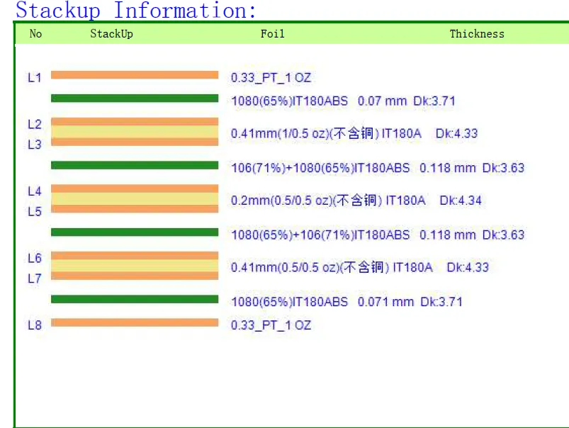
Figure 1: 8-layer stackup information
Our team micro-adjusted PP and core thicknesses based on available TG170 material inventory while keeping the final 1.6mm thickness. We sent the optimized lamination diagram for confirmation. If ignored, mismatched dielectric thicknesses could cause layer-to-layer registration shift, leading to via misalignment, drill breakout, or unreliable plating. In worst cases, this results in open circuits after thermal stress or field failures due to via cracking.
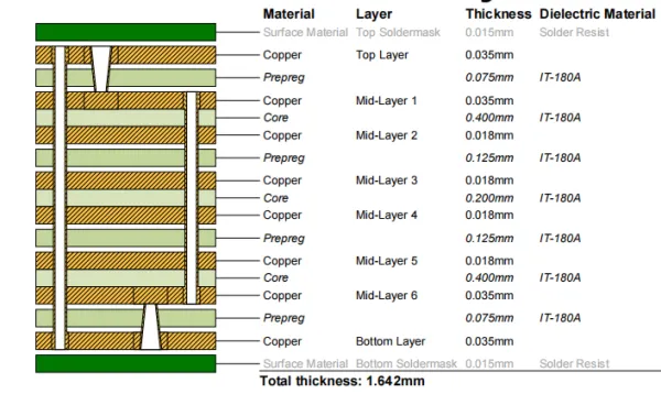
Figure 2: Layer stack legend
According to typical IPC-6012 Class 2 considerations for multilayer boards, maintaining consistent resin content and symmetric construction is critical to minimize warpage. The customer confirmed our optimized stackup, allowing us to proceed safely.
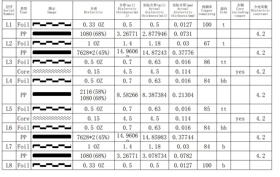
Figure 3: Optimized stackup
Process Edge Direction and Panelization Confirmation
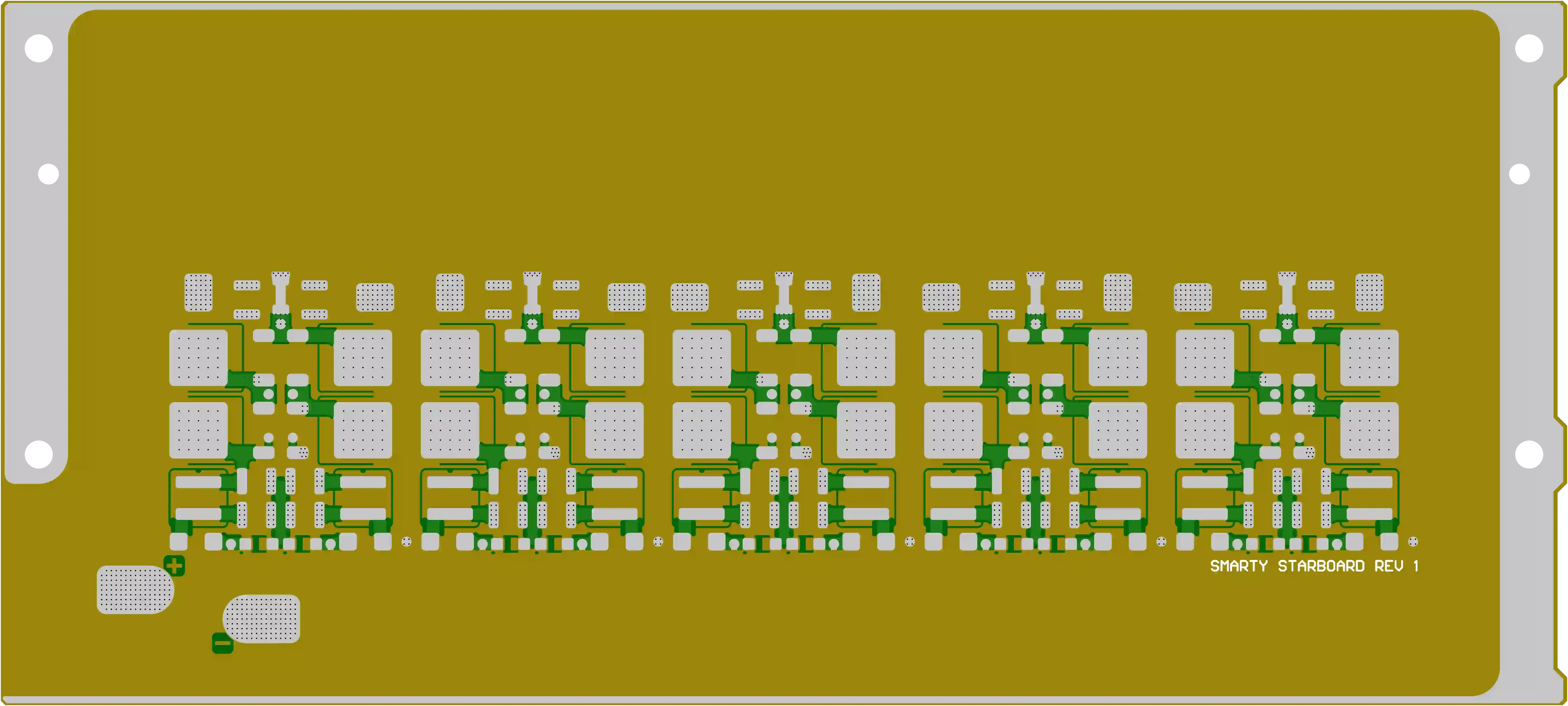
The fabrication drawing specified left-right 4mm process edges, but our standard production workflow for this panel size and V-cut requirements uses up-down orientation. Our CAM engineer identified this conflict early. We prepared a revised panelization layout and sent it for approval.
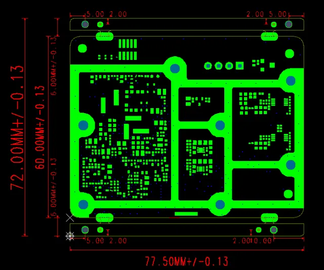
Figure 4: Revised panelization up-down layout
If we had followed the original note without clarification, the V-cut or routing could have come too close to functional copper features, risking exposed copper after depanelization. This commonly leads to edge shorting during assembly or cosmetic defects that fail IPC-A-600 inspection. Adjusting the panelization prevented these risks and maintained the required 4mm clearance.
Board Thickness Specification Conflict and Marking Requirements
Two locations in the documentation listed conflicting finished board thickness values. We raised this for confirmation to avoid tooling errors. Additionally, the customer required specific characters and production numbering on the solder mask (white), but the original Gerber/ODB files lacked the actual legend data. We added the markings as copper-open on top layer solder mask per the reference image and confirmed the font and placement.
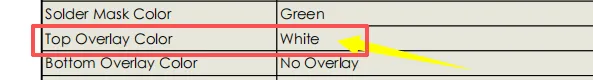
Figure 5: Required top overlay color: white
Isolated or poorly defined markings can cause solder mask registration issues or legend peeling. For the pads with potential burrs noted in the files, we confirmed production with exposed copper and minor burr allowance, which is acceptable for ENIG but requires customer sign-off to match expectations.
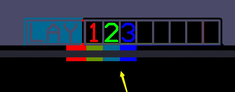
Figure 6: Confirmed production with exposed copper and minor burr allowance
Manufacturing Risks and DFM Insights
This case highlights several recurring DFM pain points in 8-layer designs with buried vias. Designers often specify process edges without considering factory standard panelization direction, leading to unnecessary EQ rounds. Similarly, incomplete legend data or conflicting thickness notes force back-and-forth communication that delays production starts.
Ignoring stackup feasibility for buried vias could have caused severe registration problems, resin voids, or delamination under reflow. Our adjustments protected yield while staying within TG170 material capabilities. Copper balancing near panel edges and proper via spacing relative to V-cut lines are critical to avoid short circuits or copper peeling after mechanical forming.
How the Engineering Team Resolved the Issues
Our CAM team prepared revised panelization drawings, optimized lamination diagrams, and temporary Gerber additions for markings. After receiving customer confirmations on all points, we updated the production data accordingly. The ODB files were regenerated with corrected layer mapping and stackup.
To reduce risk, we also verified the 0.1mm hole plating process parameters and confirmed 100% flying probe coverage. These steps ensured the board met both electrical and mechanical requirements before releasing to the production floor.
Final Manufacturing Outcome
All engineering questions were clarified and confirmed by the customer. The optimized stackup and panelization were approved, markings added as specified, and the order released for production with updated tooling. The job proceeded without further issues under the standard 9-day lead time.
Key Takeaways for PCB Designers
- Provide complete legend data in Gerber or ODB format when requiring specific characters or production numbers on solder mask.
- Ensure board thickness specifications are consistent across all documents and drawings.
- Confirm stackup feasibility with your manufacturer early when using buried or blind vias in multilayer builds.
- Clearly indicate process edge direction but allow flexibility for factory-standard panelization to optimize material utilization.
- Define via types and depths explicitly in fabrication notes for complex HDI-like structures.
- Include reference images or detailed callouts for any special markings or mechanical requirements.
FAQ
Q: Why was stackup optimization necessary for the 2-7 buried via?
A: Standard single-core lamination often cannot achieve reliable registration and resin fill for buried vias spanning multiple layers. Using two cores with adjusted PP thickness ensures better control over dielectric spacing and reduces the risk of via misalignment or voids.
Q: What happens if process edge direction conflicts are ignored?
A: V-cut or routing may violate minimum clearance to copper features, resulting in exposed copper on board edges after depanelization and potential short circuits during assembly or testing.
Q: Why do factories ask for confirmation on solder mask markings?
A: Original design files often lack the actual artwork for requested text or logos. Adding them manually requires verification of placement, font, and opening type (copper exposed or covered) to avoid legend defects or registration errors.
Q: How important is consistent board thickness specification?
A: Conflicting notes can lead to wrong lamination parameters or incorrect final thickness, affecting impedance, assembly fit, and mechanical strength. CAM review catches these to prevent scrap.
Q: Can ODB++ files that fail to open still be used for production?
A: Usually not without repair or conversion. Our team works with customers to resolve file issues quickly, often requesting native CAD exports or corrected Gerbers for accurate CAM processing.