In January 2026, we received an 8-layer impedance-controlled PCB order sized 275 × 300 mm with 1.6 mm finished thickness. The design included TG170 FR-4 material, ENIG finish, resin-plugged vias, and V-CUT + routing panelization. Although the layer count and impedance requirements were standard for high-speed applications, the CAM review revealed several critical DFM conflicts that required detailed customer clarification.
Impedance-controlled multi-layer boards with dense layouts and mixed via treatments frequently trigger engineering questions. Our CAM team identified multiple manufacturability gaps related to solder mask, hole definitions, and stackup that could have caused serious production and assembly issues if ignored.
8-Layer Impedance-Controlled PCB Order Specifications and Panelization
This was an 8-layer FR-4 TG170 PCB ( #FR4-20260124-031 ) with 1 oz copper on inner and outer layers, 1.6 mm thickness, and ENIG surface finish. Minimum hole size reached 0.15 mm. The board required impedance control and resin plugging for vias. Panelization was customer self-panel in 2×2 format with V-CUT + routing separation. Order quantity was 20 pcs (5 sets). 100% flying probe testing was specified.
The combination of tight tolerances, impedance requirements, and dense pad layout made thorough DFM review essential before releasing to production.
Critical DFM Issues Identified in 8-Layer Impedance PCB CAM Review
1. Tight Hole-to-Pad Spacing and Solder Mask Bridge Issues
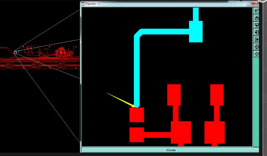
We noticed multiple locations where 0.4 mm holes and pads had insufficient spacing. Our process capability does not allow reliable solder mask bridges in these areas. Additionally, several other pad groups showed spacing below our minimum threshold for mask bridge formation.
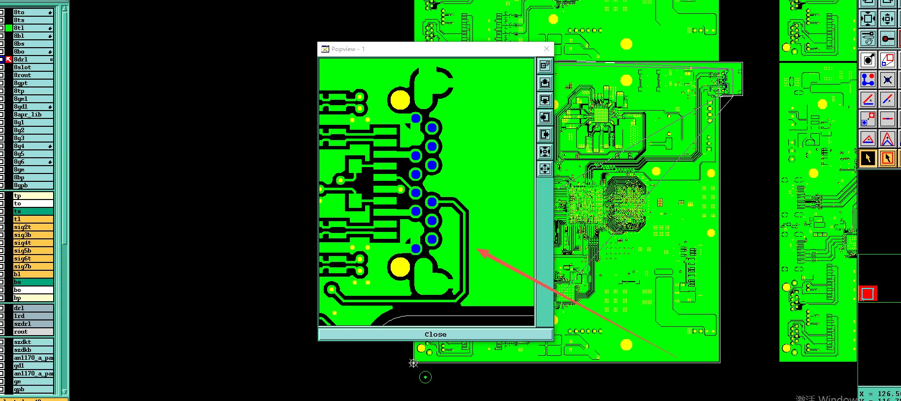
Figure 1: 0.4 mm holes and pads had insufficient spacing
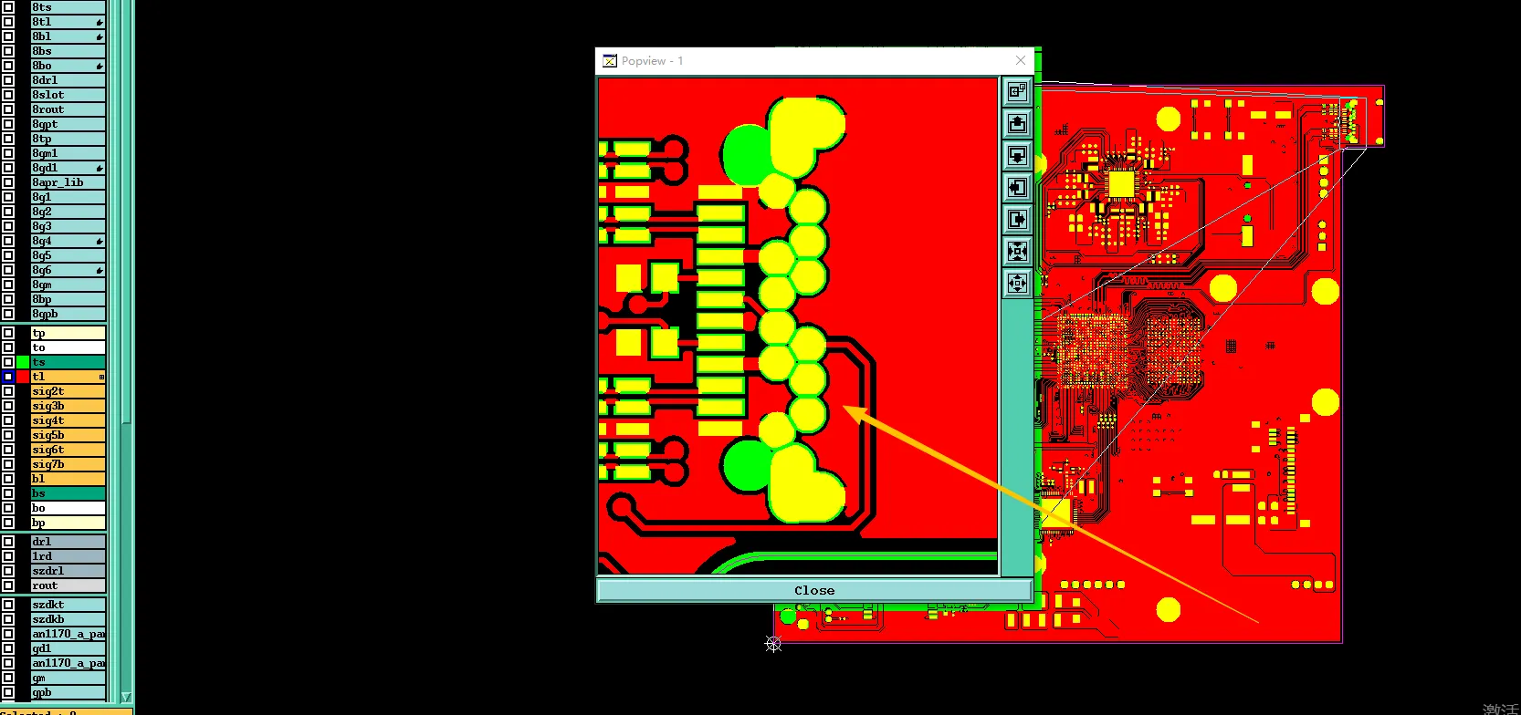
Figure 2: 0.4 mm holes and pads had insufficient spacing
Our CAM engineer flagged these areas with annotated images and proposed proceeding without bridges in the tightest zones. We asked the customer for confirmation.
If ignored, solder mask would fail to form proper bridges, leading to solder shorts during assembly, exposed copper, or mask peeling. In high-volume production this often results in significant yield loss and costly rework.
| Parameter | Minimum Requirement | Risk if Insufficient |
|---|---|---|
| Pad-to-Pad Spacing | Sufficient for bridge after compensation | Solder shorts during SMT |
Table 1: Solder Mask Bridge Requirements for Tight Pads
2. Impedance Stackup and Control Line Clarification
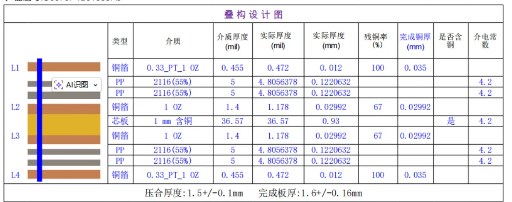
The customer provided an impedance table, but our review found that several referenced lines were missing or unclear in the design data. We prepared a complete stackup calculation using our standard FR-4 TG170 material and sent the detailed impedance report for confirmation.
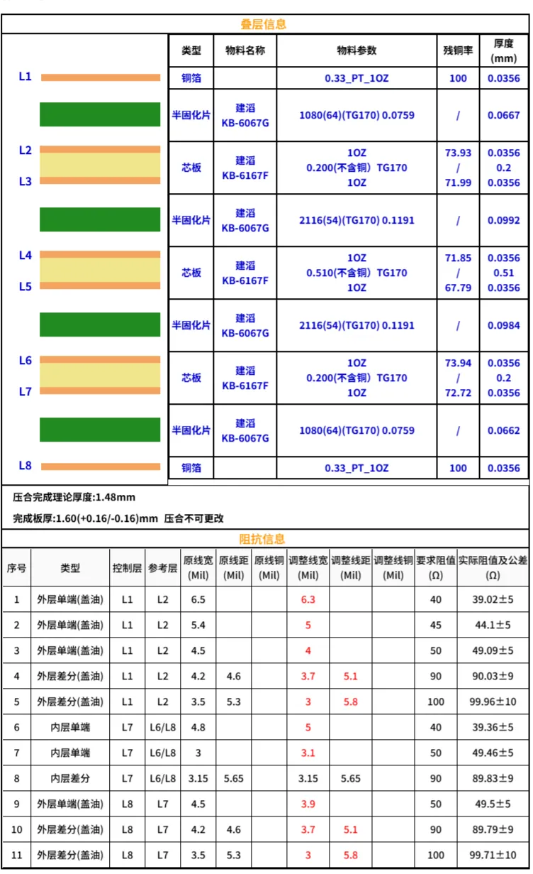
Figure 3: our standard FR-4 TG170 material and the detailed impedance report
After reviewing the 8-layer PCB stackup, we adjusted dielectric thicknesses to achieve the target 90Ω and 100Ω values while maintaining overall board thickness. We asked the customer to verify which specific lines required strict control.
Without proper confirmation, the finished boards could have impedance values outside tolerance, causing signal integrity problems, reflections, or complete functional failure in high-speed circuits.
3. Solder Mask Openings on Slots and Vias
Several slots in the original data had no solder mask openings, which would allow ink to flow into the slots during printing. Some vias also showed oversized openings that risked exposed copper after ENIG plating.
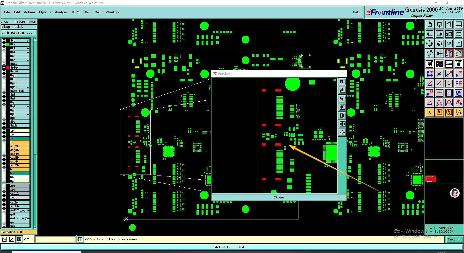
Figure 4: no solder mask openings
We raised EQs with clear screenshots and recommended appropriate mask adjustments to prevent ink intrusion and copper exposure.
If left unaddressed, ink in slots would affect mechanical fitment, while exposed copper around vias could lead to tin bridging, corrosion, or poor solderability.
4. Hole Definitions and Marking Placement
Many holes were drawn the same size as their pads. We proposed treating them as NPTH and sought confirmation. We also clarified fiducial arc features appearing on multiple layers and provided updated marking placement (year-week format) for customer approval.
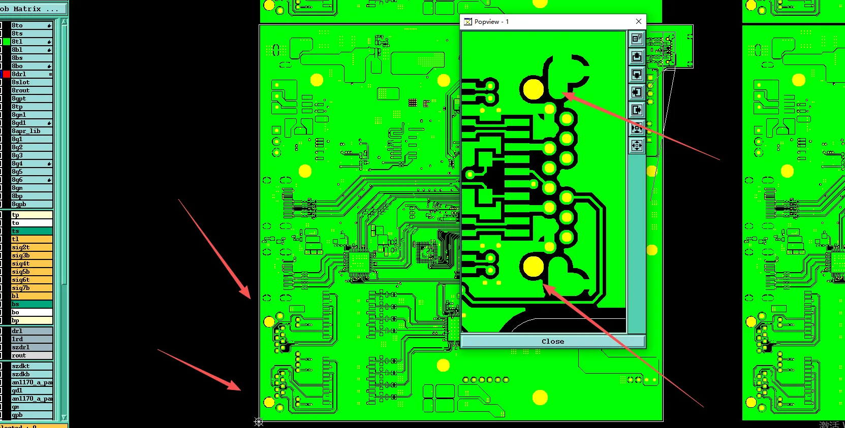
Figure 5: Many holes were drawn the same size as their pads
This ambiguity in hole definitions is common when designers do not explicitly distinguish between plated and non-plated holes. Treating same-size holes as PTH by default could lead to unintended copper plating inside non-functional holes, increasing the risk of shorts or unnecessary process complexity. Conversely, misclassifying PTH as NPTH would prevent proper electrical connectivity. Fiducial arcs on multiple layers also required clarification to avoid duplicate or conflicting features that could confuse alignment during drilling and registration.
For traceability, we recommended standard year-week date code marking in a non-critical area. The customer confirmed the hole classifications, fiducial handling, and marking placement. These clarifications ensured accurate hole plating, proper mechanical features, and reliable lot tracking throughout production and potential field service.
Key Manufacturing Risks in Dense 8-Layer Impedance PCB Production
This case clearly shows how dense layouts combined with impedance requirements create multiple DFM challenges. Tight hole-to-pad spacing is one of the most frequent triggers for solder mask defects. Missing or unclear impedance reference lines often lead to stackup mismatches, while inconsistent mask openings on slots and vias commonly cause both cosmetic and functional failures.
Designers frequently push minimum spacing rules without considering actual mask and plating capabilities, resulting in repeated data revisions and production delays.
How the Engineering Team Resolved the Issues
Our engineering team prepared detailed comparison files, annotated screenshots, and revised production data for each point. After several rounds of clarification, the customer approved the impedance stackup, solder mask strategy, hole definitions, and marking placement. We updated the production files accordingly and confirmed the final panel data.
To reduce manufacturing risk, our CAM engineer optimized the mask openings and ensured consistent treatment across all vias and slots.
Successful Production Release After Full DFM Alignment
All engineering questions were resolved and approved by the customer. The production data passed final DFM review and was successfully released for fabrication with optimized impedance parameters and mask settings.
Essential DFM Guidelines for 8-Layer Impedance-Controlled PCB Design
- Provide complete and clear impedance tables with reference layers and target values early in the project.
- Maintain sufficient spacing around holes and pads to allow reliable solder mask bridges (typically ≥ 7-8 mil).
- Clearly define solder mask openings for slots and vias to prevent ink intrusion or exposed copper.
- Coordinate hole sizes and pad definitions carefully — avoid making holes the same size as pads unless intentionally NPTH.
- Include all mechanical features (fiducials, markings, outlines) consistently across relevant layers.
- Verify stencil layer handling separately as CAM engineers normally do not modify it.
- Review manufacturer stackup proposals thoroughly when impedance control is required.
| Area | Recommendation |
|---|---|
| Impedance | Provide clear targets and reference layers |
| Solder Mask | Ensure bridge compatibility on tight pads |
| Vias/Slots | Define openings clearly |
Table 2: 8-Layer Impedance PCB DFM Checklist
FAQ
Q1: Why can't solder mask bridges be formed on very tight pad spacing?
A1: When spacing falls below the process minimum, the mask ink cannot reliably separate pads, leading to shorts or incomplete coverage during assembly.
Q2: What happens if impedance lines are not clearly identified?
A2: The manufacturer may miss controlled lines or calculate incorrect values, resulting in out-of-tolerance impedance and signal integrity issues.
Q3: Should slots have solder mask openings?
A3: Yes. Without openings, solder mask ink will flow into the slots, affecting mechanical assembly and appearance.
Q4: Why do factories ask for stackup confirmation on impedance boards?
A4: Material Dk values and dielectric thicknesses directly affect impedance. Confirmation ensures the final board meets the specified electrical requirements.
Q5: What is the risk of oversized solder mask openings?
A5: Oversized openings can leave copper exposed after surface finish, increasing the chance of tin bridging, oxidation, or assembly defects.