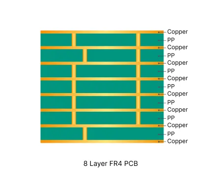
8 Layer FR4 PCB Production Record #FR4-20260124-031
| Parameter | Value | Parameter | Value |
|---|---|---|---|
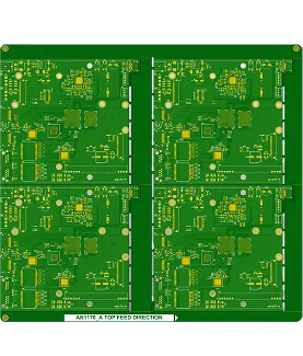
| PCB Type | FR4 PCB | Quantity | 5 pcs |
| Layers | 8 Layers | Board Type | Panel PCB |
| Dimensions | 275 x 300 mm | Copper Weight | 1oz |
| Thickness | 1.6 mm | Min Track / Spacing | 3/3mil |
| Surface Finish | ENIG (Immersion Gold) | Min Hole Size | 0.15mm |
| Solder Mask | Green | Silkscreen | White |
| Stack-up | Custom | Impedance Control | Yes |
This 8-layer FR-4 board (275 × 300 mm, 1.6 mm finished thickness) was built in a quantity of 20 pieces (5 sets) using Shengyi S1000-2M TG170 material with 1 oz copper on inner and outer layers. Key features included 0.15 mm minimum holes, 3 mil line width/space, ENIG surface finish, impedance control, and resin-plugged vias. Production used 2×2 panelization with V-CUT and routing, completed in 11 days with 100% flying probe testing and delivery of electrical test reports plus quality certificates.
DFM review addressed multiple points to ensure manufacturability. Stack-up and impedance lines were confirmed and calculated against the provided table, with adjustments made for the available material. Several via and slot openings required clarification to prevent solder mask ink intrusion into holes. Tight pad and hole spacings (some 0.4 mm holes) were evaluated for solder mask bridge capability; bridges were omitted where process limits could not be met after customer confirmation. Solder mask window sizes, PTH/NPTH treatments, outline alignment with drill data, and fiducial features were all verified. Production markings including date code were added per specification, and stencil layer handling was clarified as customer responsibility.
All files were confirmed before release. The finished boards met impedance targets, dimensional tolerances, and electrical requirements with reliable via plugging and solder mask coverage. For detailed discussion of the impedance stack-up confirmation and solder mask bridge limits in this controlled build, refer to the related engineering case.
These boards integrate multiple microvia layers to support complex routing and high signal density in advanced electronics.

In-depth guide to the most frequent Engineering Queries (EQ) and DFM issues in Multilayer FR4 PCB (4/6/8+ layers) production. Real factory insights on stack-up confirmation, impedance control, copper balance, inner layer design, via treatment, registration, and practical prevention strategies.
| Order ID | PCB Type | Layers | Dimensions | Solder Mask | Surface Finish | Quantity | Action |
|---|---|---|---|---|---|---|---|
| FR4-20260630-014 | FR4 PCB | 2 | 126 x 145 | Green | ENIG (Immersion Gold) | 10 | View detail |
| FR4-20260529-059 | FR4 PCB | 2 | 147.3 x 53.8 | Green | ENIG (Immersion Gold) | 5 | View detail |
| FR4-20260520-046 | FR4 PCB | 2 | 94.21 x 275 | Green | ENIG (Immersion Gold) | 75 | View detail |


