8 Layer FR4 PCB Production Record #FR4-20260504-095
| Parameter | Value | Parameter | Value |
|---|---|---|---|
| PCB Type | FR4 PCB | Quantity | 10 pcs |
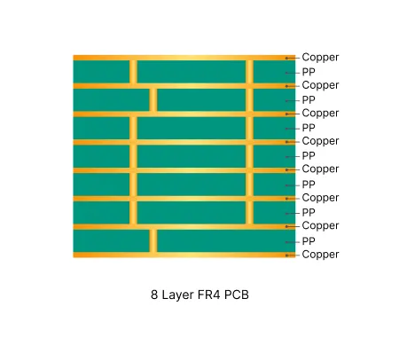
| Layers | 8 Layers | Board Type | Panel PCB |
| Dimensions | 281 x 100 mm | Copper Weight | 1oz |
| Thickness | 1 mm | Min Track / Spacing | 4/4mil |
| Surface Finish | ENIG (Immersion Gold) | Min Hole Size | 0.3mm↑ |
| Solder Mask | Green | Silkscreen | None |
| Stack-up | Custom | Impedance Control | No |
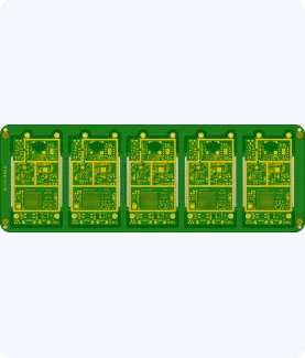
This 8-layer FR-4 board (281 × 100 mm, 1.0 mm finished thickness) was manufactured in a quantity of 50 pieces (10 sets) using Shengyi S1000H TG150 material with 1 oz copper on inner and outer layers. The design included 0.3 mm minimum holes, 4 mil line width/space, ENIG surface finish, blind vias, and customer-supplied 1×5 panelization. Production was completed in 30 days with 100% flying probe testing and full electrical test reports plus quality certificates delivered.
DFM review required multiple clarifications. Stack-up was constructed from available TG150 halogen-free cores and prepregs after customer approval. Tight 2 mil SMD pad spacings were addressed by confirming solder mask bridge capability limits and implementing customer-specified coverage adjustments on test points (0.15 mm overlap on Popview 2, removal on Popview 1). Via windowing followed the original Gerber (mixed covered and open designs) after confirmation, with attention to potential exposed copper risks. NSMD BGA pads were processed per design to improve pad adhesion and reduce cratering risk. Panelization was optimized per customer PDF reference, adding tool holes, optical fiducials, and process edge copper while adjusting stamp hole positions and bridge sizes to minimize breakout burrs and ensure clean depanelization.
Standard process controls were applied for ENIG thickness, warpage, solder mask thickness, and dimensional tolerances. All boards passed final inspection to IPC Class 2. For detailed discussion of the NSMD BGA solder mask handling and blind via DFM considerations in this build, refer to the related engineering case.
These boards integrate multiple microvia layers to support complex routing and high signal density in advanced electronics.

In-depth guide to the most frequent Engineering Queries (EQ) and DFM issues in Multilayer FR4 PCB (4/6/8+ layers) production. Real factory insights on stack-up confirmation, impedance control, copper balance, inner layer design, via treatment, registration, and practical prevention strategies.
| Order ID | PCB Type | Layers | Dimensions | Solder Mask | Surface Finish | Quantity | Action |
|---|---|---|---|---|---|---|---|
| FR4-20260520-046 | FR4 PCB | 2 | 94.21 x 275 | Green | ENIG (Immersion Gold) | 75 | View detail |
| FR4-20260516-065 | FR4 PCB | 4 | 119 x 98 | Green | ENIG (Immersion Gold) | 20 | View detail |
| FR4-20260515-068 | FR4 PCB | 14 | 244 x 267 | Green | ENIG (Immersion Gold) | 10 | View detail |


