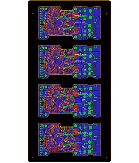
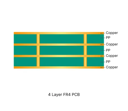
4 Layer FR4 PCB Production Record #FR4-20260427-053
| Parameter | Value | Parameter | Value |
|---|---|---|---|
| PCB Type | FR4 PCB | Quantity | 125 pcs |
| Layers | 4 Layers | Board Type | Panel PCB |
| Dimensions | 96.1 x 187 mm | Copper Weight | 3oz |
| Thickness | 1.2 mm | Min Track / Spacing | 6/6mil↑ |
| Surface Finish | ENIG (Immersion Gold) | Min Hole Size | 0.3mm↑ |
| Solder Mask | Green | Silkscreen | None |
| Stack-up | Custom | Impedance Control | No |
This 4-layer heavy copper FR-4 board (96.1 × 187 mm, 1.2 mm finished thickness) was produced in a batch of 500 pieces (125 sets) using Shengyi S1000H TG150 material with 3 oz copper on both inner and outer layers. The design featured 0.3 mm minimum holes, 6 mil line width/space, ENIG surface finish, resin-plugged vias, and V-CUT plus milling for depanelization. Production followed a 21-day lead time with 100% flying probe testing, electrical test reports, quality certificates, and microsection analysis delivered.
DFM review addressed several critical points. SMT pads positioned close to the heavy copper board edge risked partial removal during V-CUT; pad-to-edge clearances were verified and confirmed. Four plated slots missing from the latest data were restored per the original PLATED_MILLING file. Solder mask openings were adjusted per customer instructions—full pad size for connector holes and original pad size plus 1 mil for others to compensate for ink flow—while confirming resin plugging scope for all vias including any vent holes. Stack-up was built from available cores and prepregs after customer approval, with L3 copper network connectivity clarified before release. Production numbering and date code marking were added on the process edge and top solder mask respectively for traceability.
All plated slots were executed as specified with copper. The final boards passed electrical and microsection requirements with consistent copper thickness and reliable via fill. For detailed handling of the V-CUT pad damage risk and plated slot clarifications in this 3 oz heavy copper build, refer to the related engineering case.
Standard multilayer solution offering practical routing density and controlled impedance for industrial and consumer electronics.

In-depth guide to the most frequent Engineering Queries (EQ) and DFM issues in Multilayer FR4 PCB (4/6/8+ layers) production. Real factory insights on stack-up confirmation, impedance control, copper balance, inner layer design, via treatment, registration, and practical prevention strategies.
| Order ID | PCB Type | Layers | Dimensions | Solder Mask | Surface Finish | Quantity | Action |
|---|---|---|---|---|---|---|---|
| FR4-20260630-014 | FR4 PCB | 2 | 126 x 145 | Green | ENIG (Immersion Gold) | 10 | View detail |
| FR4-20260611-021 | FR4 PCB | 2 | 245.59 x 304.79 | White | HASL Lead Free | 1400 | View detail |
| FR4-20260605-042 | FR4 PCB | 4 | 65 x 100 | Green | HASL Lead Free | 5 | View detail |


