Typical Specification Range
| Parameter | Mid to high density multilayer designs |
|---|---|
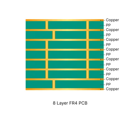
| Layer count | 8 layers |
| Material type | FR4, High Tg FR4 |
| Surface finish | ENIG, HASL, Immersion Silver |
| Thickness | 1.0mm to 3.0mm |
| Solder mask | Green, black, red, white, yellow, blue, purple, matte black, matte black |
| Copper thickness | 1oz to 2oz |
| Special features | Impedance control, blind vias, buried vias |
Manufacturing Process Insights
Lamination: Manufacturing 8-layer FR4 PCBs involves greater complexity than lower layer count boards due to multiple lamination cycles, the integration of blind and buried vias, and stricter requirements for dimensional stability and electrical performance. Based on our production experience, several process stages require focused control to ensure consistent quality and yield. Multi-stage Lamination 8-layer boards are typically built using two or three lamination cycles, depending on the stackup design. Each lamination introduces risks related to layer registration, resin flow, and thermal stress. We pay close attention to temperature ramp rates, pressure distribution, and vacuum levels during pressing to minimize voids and delamination. Symmetric copper distribution across the stackup, combined with copper thieving patterns, is applied to reduce warpage caused by repeated thermal cycles.
Drilling: Drilling and Via Processing Drilling operations in 8-layer boards include through holes, blind vias, and buried vias. Blind and buried vias require more precise depth control and specialized desmear processes, particularly when high Tg materials are used. We implement staged drilling strategies and optimize parameters according to via type and material characteristics to maintain hole wall quality and ensure reliable plating adhesion.
Plating: Plating and Metallization Higher layer counts result in increased aspect ratios, making uniform copper deposition inside vias more challenging. Our process focuses on controlling both electroless and electrolytic plating steps to achieve consistent barrel thickness. Regular cross-section analysis is performed to verify plating quality, especially for blind and buried vias where plating defects can be difficult to detect through standard electrical testing.
Surface Finish: Surface Finish Selection and Application ENIG is the predominant surface finish for 8-layer FR4 boards, especially when fine-pitch components or BGAs are present. We adjust nickel and gold thickness based on copper weight, assembly requirements, and shelf-life expectations. For boards with higher copper weights or specific thermal demands, alternative finishes such as Immersion Silver or HASL may be recommended after evaluating solderability and long-term reliability needs.
Manufacturing Order Profile
| Order Quantity | Order Proportion | Estimated Price Level | Typical Lead Time |
|---|---|---|---|
| Prototype (<=30 pcs) | 61% | From $110 | From 4 days |
| Small volume (30-200 pcs) | 26% | From $130 | From 5 days |
| Mass production (>200 pcs) | 13% | From $200 | From 6 days |
Manufacturing Challenges & Process Optimization
Design Considerations
Related Products
Common Applications
PCB Solution for Power Supply
Maximize power density and safety with AIVON’s specialized power supply PCBs. Engineered to handle high currents and thermal loads, our designs feature thick copper, thermal vias, and strict high-voltage isolation. We ensure superior efficiency and robust stability for applications ranging from chargers to industrial converters.
PCB Solution for Automotive Electronics
AIVON automotive electronics PCBs are designed for demanding vehicle environments. They withstand extreme temperatures, vibration, and harsh conditions, supporting ECUs, ADAS, infotainment, and EV modules. Featuring multilayer, rigid-flex, and high-frequency designs, AIVON PCBs meet IATF 16949 standards for safe and reliable automotive performance.
PCB Solution for Industrial Control
AIVON engineers rugged PCBs for industrial control systems demanding unwavering reliability in harsh environments. Featuring high-Tg materials, heavy copper, and conformal coatings, our solutions withstand extreme heat and vibration. We ensure superior signal integrity and long-term stability for PLCs, robotics, and drives, maximizing your operational uptime.
Real Production Records
| Order ID | PCB Type | Layers | Dimensions | Solder Mask | Surface Finish | Quantity | Action |
|---|---|---|---|---|---|---|---|
| Loading... | |||||||
View More Engineering Resources
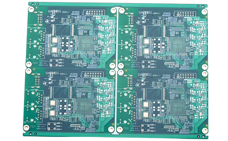
Why Choose AIVON for 8 Layer FR4 PCB?
AIVON manufactures 8 layer FR4 PCBs with strict multilayer lamination control and high-precision registration to ensure excellent interlayer alignment. Advanced inner layer imaging, copper plating, and vacuum pressing deliver consistent impedance, reliable via reliability, and tight overall tolerances for complex, high-density applications.

FR-4 PCB Design for Wearable Technology: Balancing Size, Weight, and Performance
Explore FR-4 PCB design for wearable technology: Master miniaturization, low-power layouts, flexible FR-4, sensor integration, Bluetooth optimization, and fitness tracker specifics. Achieve lightweight boards under 5g with IPC-4101C standards—key for 2025 smartwatches.
Read More
FR-4 PCB Design Fundamentals: A Beginner's Step-by-Step Guide
Learn the basics of FR-4 PCB design, from material understanding to creating single and double-layer boards using popular software like KiCad, Eagle, and Altium.
Read More


