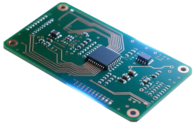
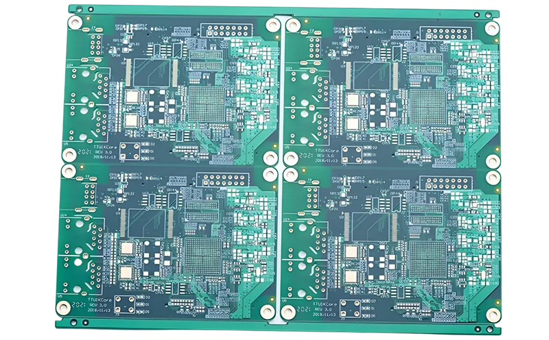
Discover how AIVON manufactures Thick FR4 PCBs, including increased board thickness control, mechanical reliability requirements, fabrication processes, manufacturing challenges, and real production experience from customer orders.
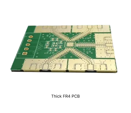
| Parameter | Typical Range |
|---|---|
| Layer count | 2-24 layers |
| Material type | FR4, High Tg FR4 |
| Surface finish | ENIG, Lead-free HASL, OSP |
| Thickness | 2.0-4.0mm |
| Solder mask | Green, black, matte black, matte green |
| Copper thickness | 1oz to 6oz |
| Special features | Symmetrical construction, controlled impedance, thermal vias |
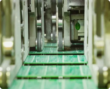
Material Preparation & Lamination Thick FR4 cores and multiple prepregs are stacked and laminated under carefully controlled heat and pressure. Heat transfer through the thicker material is slower, so press parameters are optimized to ensure complete resin flow, minimize voids and maintain uniform thickness across the panel.
High-Aspect-Ratio Drilling CNC drilling creates through-holes in material that is often 2.0–4.0 mm or thicker. Drill parameters, bit geometry and entry/backup materials are specially tuned to control hole-wall roughness, reduce drill wander and manage the elevated aspect ratio (depth-to-diameter).
Desmear & Plating Chemical desmear is intensified to remove resin smear from deep hole walls. Electroless and electrolytic copper deposition must achieve reliable coverage through the full board thickness; plating uniformity becomes significantly more challenging as aspect ratio increases.
Via Tenting / Plugging Solder-mask tenting or resin plugging of high-aspect-ratio vias requires process compensation (often pre-drilling larger holes). Incomplete tenting or plugging risks ink intrusion, solder-bead entrapment or open circuits after surface finish.
Routing, Countersink & Mechanical Features Contour routing, V-scoring and precision countersinks are performed with tooling selected for thick, rigid material. Depth and angle control of countersunk holes, as well as large NPTH features, demand tighter process monitoring.
Final Inspection Cross-section analysis of high-aspect-ratio vias, thickness measurement, warpage check and mechanical feature verification ensure the thick board meets both electrical and structural requirements before shipment.
| Order Quantity | Order Proportion | Estimated Price Level | Typical Lead Time |
|---|---|---|---|
| Prototype (<=30 pcs) | 65% | From $28 | From 1 Day |
| Small volume (30-200 pcs) | 19% | From $50 | From 1 Day |
| Mass production (>200 pcs) | 14% | From $85 | From 1 Day |
| Order ID | PCB Type | Layers | Dimensions | Solder Mask | Surface Finish | Quantity | Action |
|---|---|---|---|---|---|---|---|
| Loading... | |||||||
Ensure uncompromising safety with our automotive-grade PCBs, compliant with stringent industry standards. Engineered for EVs, ECUs, and railway signaling, our boards withstand extreme vibration and thermal shock. We deliver the rugged reliability and precision required for mission-critical transportation electronics.
AIVON empowers the renewable sector with high-performance PCBs for solar inverters, wind turbines, and Battery Management Systems (BMS). Engineered to withstand high voltages and harsh outdoor environments, our boards ensure precise energy conversion. Maximize your energy harvest and storage efficiency with our reliable, robust interconnect solutions.
AIVON engineers rugged PCBs for industrial control systems demanding unwavering reliability in harsh environments. Featuring high-Tg materials, heavy copper, and conformal coatings, our solutions withstand extreme heat and vibration. We ensure superior signal integrity and long-term stability for PLCs, robotics, and drives, maximizing your operational uptime.
AIVON manufactures Thick FR4 PCBs with precise control over board thickness from 2.0mm to 3.2mm or more. Using high-quality FR4 material, advanced vacuum lamination, and stable drilling & plating processes, we ensure excellent dimensional stability, reliable via integrity, and tight overall thickness tolerance for applications requiring high mechanical strength and durability.
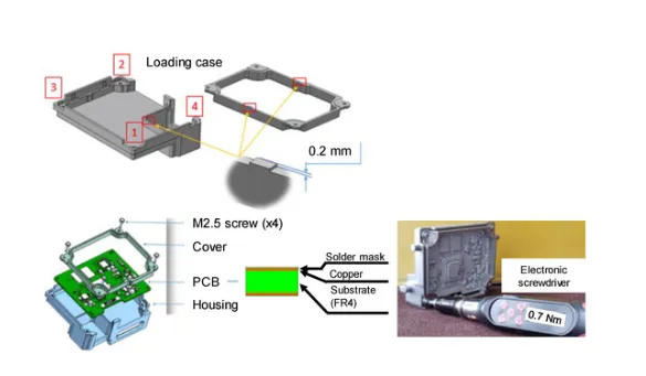
Learn advanced techniques for hybrid stack up PCB design in RF laminates. Optimize performance with FR4 combinations, CTE matching, and cost effective solutions for reliable multilayer boards in high frequency systems.
Read More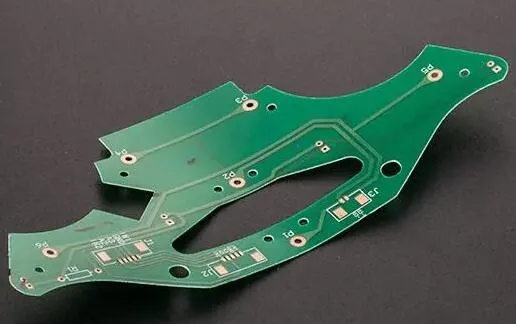
Learn the basics of FR-4 PCB design, from material understanding to creating single and double-layer boards using popular software like KiCad, Eagle, and Altium.
Read More