Typical Specification Range
| Parameter | Typical Range |
|---|---|
| Layer count | 4 layers |
| Material type | FR-4, High Tg FR-4 |
| Surface finish | ENIG, OSP, Immersion Tin |
| Thickness | 0.4mm to 3.2mm |
| Solder mask | Green, black, red, white, yellow, blue, purple |
| Copper thickness | 0.5oz to 2oz |
| Special features | Blind microvias, stacked vias, fine pitch lines |
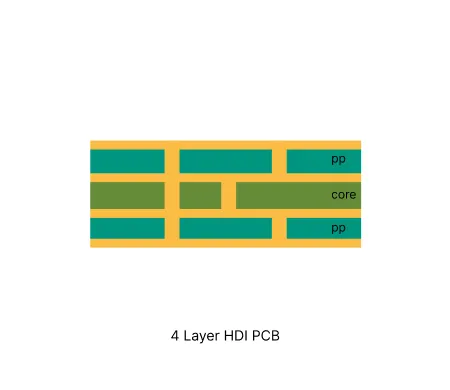
Manufacturing Process Insights
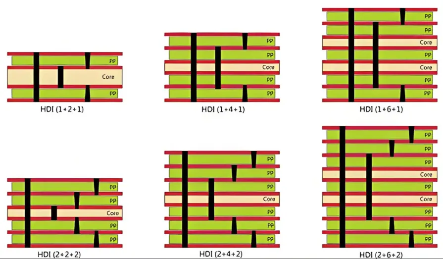
Sequential Lamination: Inner core is laminated first. Outer layers add through controlled press cycles with prepreg.
Laser Drilling: UV and CO2 lasers create microvias. Plasma desmear follows to clean via walls.
Plating Logic: Direct metallization and electrolytic copper fill microvias uniformly. Current density is tightly controlled.
Surface Finish: ENIG is preferred for fine pitch assembly reliability.
Registration control and via inspection mitigate risks throughout the process.
Manufacturing Order Profile
| Order Quantity | Order Proportion | Estimated Price Level | Typical Lead Time |
|---|---|---|---|
| Prototype (<=30 pcs) | 69% | From $180 | From 7 days |
| Small volume (30-200 pcs) | 22% | From $220 | From 8 days |
| Mass production (>200 pcs) | 9% | From $330 | From 8 days |
Manufacturing Challenges & Process Optimization
Design Considerations
Related Products
.webp)
Common Applications
PCB Solution for Industrial Control
AIVON engineers rugged PCBs for industrial control systems demanding unwavering reliability in harsh environments. Featuring high-Tg materials, heavy copper, and conformal coatings, our solutions withstand extreme heat and vibration. We ensure superior signal integrity and long-term stability for PLCs, robotics, and drives, maximizing your operational uptime.
PCB Solution for Automotive Electronics
AIVON automotive electronics PCBs are designed for demanding vehicle environments. They withstand extreme temperatures, vibration, and harsh conditions, supporting ECUs, ADAS, infotainment, and EV modules. Featuring multilayer, rigid-flex, and high-frequency designs, AIVON PCBs meet IATF 16949 standards for safe and reliable automotive performance.
PCB Solution for Transportation
Ensure uncompromising safety with our automotive-grade PCBs, compliant with stringent industry standards. Engineered for EVs, ECUs, and railway signaling, our boards withstand extreme vibration and thermal shock. We deliver the rugged reliability and precision required for mission-critical transportation electronics.
View More Engineering Resources
Why Choose AIVON for 4 Layer HDI PCB?
AIVON manufactures 4 Layer HDI PCB with laser microvia drilling, sequential lamination, and fine line imaging capability, ensuring high interconnect density, precise via alignment, and stable electrical performance in high-reliability production.
Mastering Microvias: A Comprehensive Guide to HDI PCB Design
Grasp microvia design rules, boost microvia reliability, stacked microvias setups, laser drilling microvias methods, and microvia impedance control for HDI PCB design. Engineering-focused guide covers best practices, testing, and configurations to ensure high-density board performance and fabrication success.
Read More
Advanced HDI PCB Design Techniques for Multilayer Boards
Learn advanced HDI PCB design techniques for multilayer boards. Gain insights on microvias, signal integrity, and layer stackup optimization to create compact, high performance electronics with reliable results.
Read More


